Thanks for this Georgio.This is my own interpretation of Scott's masterpiece.
Can you post a pic with what the pins of J1 & J2 do?
Also the EXACT circuit of what is on the PCB.
Hi,
I'm leaving on a business trip so it will take a couple of days before I can post the schematics. In any case, the connector pinout is:
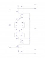
J1-1 +VCC
J1-2 NULL/COMP
J1-3 NULL
J1-4 -IN
J1-5 +IN
J1-6 COMP
J2-1 GND
j2-2 GMC
j2-3 OUT
j2-4-VCC
The NULL pins are for easy access to offset nulling on the +VCC side. The NULL/COMP pin has double duty as it also provide access to compensation for unity gain configurations. The GMC pin is the output of the gain stage / input of diamond buffer. GND is the ground plane.
Regards
Giorgio
I'm leaving on a business trip so it will take a couple of days before I can post the schematics. In any case, the connector pinout is:
J1-1 +VCC
J1-2 NULL/COMP
J1-3 NULL
J1-4 -IN
J1-5 +IN
J1-6 COMP
J2-1 GND
j2-2 GMC
j2-3 OUT
j2-4-VCC
The NULL pins are for easy access to offset nulling on the +VCC side. The NULL/COMP pin has double duty as it also provide access to compensation for unity gain configurations. The GMC pin is the output of the gain stage / input of diamond buffer. GND is the ground plane.
Regards
Giorgio
THD Construction Documentation
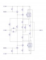
The attached files describe one possible implementation of the SW-OPA topology using primarily through-hole (THD) devices. They include a "clean" schematic, printed wiring board (PWB) layout, parts list with suggested sources and current (Apr 2013) cost data, and an LTSpice circuit file for simulation. I would appreciate helpful comments on the design, PWB layout, and documentation. This is a THD version of the package I submitted in Post #2656. Many of my comments in Post #2656 apply to this design and documentation; I won't repeat them here but I encourage you to review that previous post.
Changes, refinements, and departures from that previous effort include:
2. Circuit Design.
- The circuit includes both the input-stage anti-latchup diode, D1 and output-stage anti-latchup diodes D2 and D3.
- The external electrical interface consists of TEN connections: inverting and non-inverting inputs; signal output; the compensation node; signal ground; positive and negative supplies; returns for positive and negative supply decoupling; and the backside ground plane.
- Jumpers permit the signal ground, supply decoupling returns, and ground plane nodes to be connected or isolated.
- There is a jumper between the input and output sections of the circuit.
3. Component Selection.
- The input stage uses four BF862 JFET's in SOT-23 packages. The remaining transistors are primarily TO-92 packaged parts.
- The specified resistors are 1% thick film parts of RN60 type. These are rated for 1/2 watt power dissipation in commercial applications, and are physically larger than 1/4 watt resistors so there is plenty of space for substitute components.
- The specified bipolar transistors in the input stages are BC550 and BC560. These are long-established "workhorse" devices, readily available from several manufacturers at low cost.
- The KSA916/KSC2316 pair are used as the output drivers. The long-term availability of these devices is uncertain. I hope that alternatives can be identified.
- The actual output devices are either KSA916/KSC2316, or KSA1220A/KSC2690A (in TO-126 packages).
4. Printed Wiring Board (PWB).
- The PWB size is 3.937" X 2.444" (100 mm X 62 mm). It conforms to the "Sick of Beige" guidelines. (See "Sick of Beige Standard PCB sizes" at < http://dangerousprototypes.com/docs/Sick_of_Beige_standard_PCB_sizes_v1.0 > .)
- The PWB is a two-sided design.
- Most of the PWB bottom side is devoted to a shield plane. Jumpers can be used to connect this plane to the signal ground node, or an external node, or left floating
- The PWB's electrical interface uses ten swaged-in-place contact pins. The specified swage pins have a stand-off shoulder, preventing component leads and solder fillets from shorting to a chassis under the PCB assembly.
- All components are identified on the top-side silkscreen, although in a few cases the placement is somewhat ambiguous. Refer to the component placement diagrams in the PWB drawings for additional guidance.
- The output stage is laid out for TO-126 devices, and includes allowance for a clip-on heatsink. TO-92 devices can be used in the output stage if the leads are formed to fit the TO-126 pad spacing. This is straightforward for TO-92 devices having an ECB pinout. It will be more difficult for TO-92 devices with EBC or CBE pinouts and short insulating sleeves are suggested for the leads.
- The output devices and their drivers are physically adjacent to each other to facilitate thermal coupling.
Dale
Attachments
It's a good thing we went to different schools together. I don't know if anybody under 40 really knows what "19 inch rack chassis" means.I would be interested in a thru-hole pcb that fits inside a standard 19 inch rack chassis . . .
To help with this effort, do you have favorite TO-36 transistors to use in this design?
Dale
Hi Dale,
I see that you are at it early today. I have loaded your gerber/drill data into Gerbtool and all looks fine to me. I have not done a complete examination but considering the amount of work that you have done, I can say, very well done. I take it that you have done a few designs previously")
One small thing to point out, I see your smallest drill/FHS is 0.016". This is fine for probably most/all fabricators. One that it will be an issue with is "batchpcb.com", which has a 0.020" FSH as a minimum, so this is what I use, if I was to use them as a fab supplier. Note, I have not used them yet.
BTW, could you post the LTspice .asc file/libs, so that I can run a sim to do some learning.
If you or anyone else is/are going to do a group buy, I'd be interested in getting a couple of pcb's to test out.
P.S. I think that you managed to make it fit into a EIA rack, have to admit, I am over 40 however.
Cheers
Rick
I see that you are at it early today. I have loaded your gerber/drill data into Gerbtool and all looks fine to me. I have not done a complete examination but considering the amount of work that you have done, I can say, very well done. I take it that you have done a few designs previously
One small thing to point out, I see your smallest drill/FHS is 0.016". This is fine for probably most/all fabricators. One that it will be an issue with is "batchpcb.com", which has a 0.020" FSH as a minimum, so this is what I use, if I was to use them as a fab supplier. Note, I have not used them yet.
BTW, could you post the LTspice .asc file/libs, so that I can run a sim to do some learning.
If you or anyone else is/are going to do a group buy, I'd be interested in getting a couple of pcb's to test out.
P.S. I think that you managed to make it fit into a EIA rack, have to admit, I am over 40 however.
Cheers
Rick
It's a good thing we went to different schools together. I don't know if anybody under 40 really knows what "19 inch rack chassis" means.
To help with this effort, do you have favorite TO-36 transistors to use in this design?
Dale
2N174... fond memories.... No, but I have a CK722 laying around.
-RNM
Glad to get to the thru hole pcb - sanity for me. I'm in for some PCB's with thru hole parts. I think I can handle a couple smd's, if I have to.
Yeah, I wanted to stick with it until the job was done - but I still forgot to attach the sim files.I see that you are at it early today.
Thanks for running that check. I always use the built-in DRC and think REAL HARD before I override any squawks. I don't think any third-party tool has ever found a problem if I'm clean on the internal DRC but it never hurts to have a different set of "eyes" (human or electronic) look at a design before building it.I have loaded your gerber/drill data into Gerbtool and all looks fine to me.
I absolutely HATE going back to something after I have decided it's finished.. . . considering the amount of work that you have done, I can say, very well done.
PWB layout was never my main job but in previous incarnations (when I had a job) I have done about a dozen PWB's from scratch, and major revisions to 4 or 5 others. The only projects I've done in this or any other hobby community are here in this thread. I had one comment that my documentation packages are far too intimidating for hobbyists.. . . I take it that you have done a few designs previously
Edit the NC Drill file to call out a 20 mil hole sted 16 mil. There's only one of the things - a via that simply refused to go away no matter which way I looked at the board or how much I cussed at it. The surrounding pad is 45 mils so there is plenty of annular ring even for a hole as large as 25 mils. I'm surprised that 16 mils is outside their process spec - even the folks at ITEAD/Seeed Studio say they can do 12 mils. I'll enlarge that via on the next pass.. . . your smallest drill/FHS is 0.016" . . . "batchpcb.com", which has a 0.020" FSH as a minimum . . .
(That via was in my program library from some project I did several years ago so I don't even know which vendor's requirements it was tailored for.)
You can't please everybody all the time, and PWB hole sizes is an area where you are lucky to please more than one at a time. Of course if you order 1000's of boards at a time you can get pretty much any hole size within reason, subject to the fabricator's tolerances. When you buy prototype or short-run quantities - 100 or less - you are usually restricted to the 10 or 12 hole sizes the vendor considers "standard". But no two vendors can agree on what the "standard sizes" are. Some of them will give you the closest standard hole size and others will round up to the next largest size - usually without telling you. (OK, it's somewhere in the fine print on their web page, or the work order.) In the majority of cases, especially for prototypes or manual assembly, this is quite acceptable. If not, or if the vendor insists that your documentation must match his offering, you must select the vendor before you lay out the PWB and tailor your library, and design rules, to what he provides.
The LTSpice files I intended to include in the original package are attached. Note that I included a plot definitions file for the open-loop gain/phase probe. The circuit file is terribly cluttered with models for all the devices I experimented with. The Yahoo LTSpice User's Group strongly encourages placing device models on the schematic, to make the circuit file as portable as possible and avoid problems with directory structures, search path hierarchies, etc. I suggest that you copy these off into a separate file, park it in the same directory where the circuit file lives, and add an " .include " or " .lib " statement to the circuit file... . . could you post the LTspice .asc file/libs, so that I can run a sim to do some learning.
Is there anything like a tutorial on how to administer a group buy? I haven't seen a real paycheck in 6 months so I'm not in a position to absorb the front-end costs of creating a stockpile to be sold over many months or years.. . . going to do a group buy, I'd be interested in getting a couple of pcb's to test out.
I stumbled across those "Sick of Beige" project boards I mentioned in my post, and since the PWB had to have SOME dimensions it may as well conform to one of their standard dimensions. I put an 0.10" (2.5 mm) electrical and mechanical keep-out on all four edges, so the PCB assembly could be slid into board guides or slots of appropriate dimensions. I have noticed a few companies making enclosures based on aluminum extrusions with slots specifically intended to hold a circuit board. See, e.g., Hammond 1455 series at http://www.hammondmfg.com/pdf/1455L1601.pdf .I think that you managed to make it fit into a EIA rack . . .
Old age and treachery trump youth and enthusiasm. And don't trust anyone under 30.. . . I am over 40 however.
Dale
Attachments
I wouldnt worry about trying to please batchPCB, afaik they have recently shut their doors, or minimum changed their supplier who is much more expensive, apparently higher spec process, but priced enough higher to make it not really worthwhile when there are other services around.
great work on the documentation btw! really excellent, I prefer the SMD version and i'm looking to use more dual parts to get the size down and with 4 layer boards so cheap now, if going for small size and high quality, it just makes sense to use 4 layer. obviously its not then possible to make at home, nor as widely accessible, but thats OK for me.
one thing though and this is half question, couldnt you go up a couple sizes for trace width on critical low noise and power supply traces?
If you want them to bolt onto the new base plates and riser plates of the new diyAudio chassis' then the mounting holes should be in a multiple of 10mm in each direction, ie: 20x40, 30x40 50x50, 50x70, that sort of thing. The plates will have a grid of holes at 10mm centers in each direction. This is different than the heatsink UMS.
The Dangerous Prototypes/Sick of Beige SQUARE shapes are all just fine..
And our chassis' are FAR FROM BEIGE!
The Dangerous Prototypes/Sick of Beige SQUARE shapes are all just fine..
And our chassis' are FAR FROM BEIGE!
Last edited:
I have no idea.Is there anything like a tutorial on how to administer a group buy?
I am in the same boat, pay cheque wise, so I understand!!I haven't seen a real paycheck in 6 months, so I'm not in a position to absorb the front-end costs of creating a stockpile to be sold over many months or years.
I guess that will have to get our own fab'd.
Thanks Dale for the sim stuff and all your hard work
Rick

If everyone's onboard with this design and gives it their blessing , including Scott who seems swallowed up by his day job, and the mounting holes fit the "multiples of 10mm" standard, then diyAudio could order a batch. We've made various boards which have come out of thread collaborations, and are still refining the process..
Here's our latest thoughts:
We list it in the store as "backordered" People order and pay for whatever number of boards they want, we then have them made at a good price, better if more are ordered. When they come in, the store then automatically sends them out. Now they would be "beta" at this stage and we can't be held responsible if they need reworking or something. Pretty seamless if people are really interested.
Mark
Last edited:
I think that Dale can decide for himself what is fair.
Mark
I think that your suggestion sounds like a good idea, provided that you give some free PCB's to Dale (dchisholm), 25 free pcb's sounds like a fair suggestion.
Stein
Yes, I'd like to look at multi-device packages on the SMD version. My objective of getting down to the API2520 footprint didn't have much support but I'd like to give it a try out of principle. Motivation and interest have been lagging for several months. Knowing that there won't be a budget to construct anything I design doesn't help.. . . I prefer the SMD version and i'm looking to use more dual parts to get the size down . . .
I think every trace on the latest (THD) PWB is 15 mils. That wasn't an entirely arbitrary value:. . . go up a couple sizes for trace width on critical low noise and power supply traces?
- I chose a value that was within reason for home fabricators
- On the patterns I used for TO-92 and SOT23 devices, a 15 mil trace can be routed between pads and meet "balanced" 15 mil trace/ 15 mil space constraints. (The TO-92 pattern itself has it's own trace/space problems, but that's another topic.)
- A quick eyeball scan of the PWB seems to show that, except for the segments running between transistor pads, traces can be universally increased to 20 mils or even 25 mils, though several segments will need to be nudged around or re-mitered to meet clearance constraints.
- The only critical low-noise nodes are the gate leads on the input BF862 pair. The signals in the drain-source circuit of these devices have already been boosted well above device noise by the transconductance of the input devices.
- Trace width shouldn't have significant influence on noise performance. If anything, wider traces will increase stray coupling capacitance and increase noise susceptibility.
For power traces, my thinking is based on:
- Except for the output devices, no trace or component carries more than 10 mA, maximum.
- By conservative PWB layout criteria, a 15 mil trace can carry 1 amp without compromising electrical performance. That gives 99% margin between operating levels and trace rating.
- The output transistor collector-emitter circuits might carry as much as 50 mA (high output drive version). This is still 95% margin but I will increase these traces to 25 mil or more on the next rev.
Dale
honestly I think it would be pretty hard to compete with the likes of iTEAD unless you use the bulk buying power to get 2oz copper, gold plate (neither really needed) the current format we can get 10 pieces 100x100mm for $24 total
as far as the changes you pretty much covered it, the input and output nodes. the thinking comes from clock circuits, the wider the trace (within reason) the better. and I dunno, I just tend to follow that where I can, when it doesnt cause layout compromises I use signal traces that equal the pin size and I prefer power planes to power traces for low impedance. its just how I roll, the comment was meant to encourage discussion not say my way is better.
i'm pretty darn sure that we can throw together and manage you a couple parts kits and PCBs for your trouble...
Last edited:
being broke is no fun at all... I can kick in some funds to get it going.... thru hole version.
drop a note to me if I can help.
Thx-RNMarsh
Been quiet too long.... What's the status?
-RNM
Last edited:
- Home
- Source & Line
- Analog Line Level
- Discrete Opamp Open Design