I have found the magazine...
... with the original article about the DIGI-125:
http://www.americanradiohistory.com/Archive-Electronics-Today/Australia/80s/ETI-1989-05.pdf
May 1989 edition from this another link:
ETI: Electronics Today International. Australian edition of this
international electronics and hobbyist magazine.
BR.
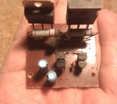
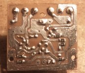
I have now built several of these modules with zero success. I started with the original schematic, then tried the rodded version rawbas posted. The last at least had output, though heavily distorted. I thought maybe my ebay bought transistors may be culprit but testing the buggers in a joule thief circuit with scope between collector and emitter revealed nearly identical output with each bc556 transistor I dropped into the socket.
I am using + - 30v on the rails, saw mention of issues with LTP a couple pages back, but being new to this I am not quite sure what I need to do to sort out issues there, nor how to set up the LTP itself and test the standalone differential pair using a single scope.
Would adding a current mirror to the differential pair add stability to knockoff components if this is the issue?
Measuring the voltage drop, I have a 1 volt drop from rail voltage to the other end of 4k7, but 32.4 volt drop to the other end of 47k feeding the LTP. 0.5volts...
Last edited:
inductance issue?
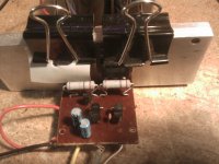
So after taking some measurements and looking over my topology, I am drawing a fair conclusion that the 1n4148 diode located directly beside the 1k input resistor may be inducting the .5 volts to the base of Q1 causing DC offset of my long tail pair.
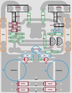
I did a little drawup for this to be constructed on perfboard, trying to keep the layout as compact as possible. I started a new build with only the differential pair and VAS thus far, plan to power it up as is and take some measurements.
So after taking some measurements and looking over my topology, I am drawing a fair conclusion that the 1n4148 diode located directly beside the 1k input resistor may be inducting the .5 volts to the base of Q1 causing DC offset of my long tail pair.
I did a little drawup for this to be constructed on perfboard, trying to keep the layout as compact as possible. I started a new build with only the differential pair and VAS thus far, plan to power it up as is and take some measurements.
Attachments
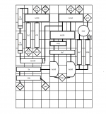
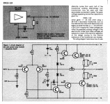
Original schematic.
I have constructed the circuit from Muff's from post #70 and tweaked some as I mentioned on post #132.
Can you measure the voltages of your transistor Vbe, base to emitter pins?
they should be around 0.5v to 0.7V.
If you have constructed the amp using the PCB layout you have posted, try reducing the 150pf (Cdom) to 56pf to 100pf.
I have encountered LPT imbalance when I have constructed the circuit, check and double check if they are properly connected, probably one or more devices has issues or already damaged, also be mindful of your groundings.
I suggest to post the circuit you have constructed and the corresponding measured voltages you have mentioned.
Last edited:
LTP balance is perfect when:
1. Base to ground T1 resistor = base to output T2 resistor
2. Both legs are set up for equality and then supply set up for 2xL1/L2.
3. Both Vbe on the two input transistors are identical.
4. Both beta on the two input transistors are identical, and
5. Both T1 and T2 are thermally bonded.
So, it's difficult to achieve this. If you can, H2 and H4 are neutralised, and only H3 is evident. OTOH, if the LTP is NOT balanced, and it usually is not, then H2 should be higher than H3. Some prefer that sound rather than H3 dominant.
Hugh
LTP balance is perfect when:
1. Base to ground T1 resistor = base to output T2 resistor
2. Both legs are set up for equality and then supply set up for 2xL1/L2.
3. Both Vbe on the two input transistors are identical.
4. Both beta on the two input transistors are identical, and
5. Both T1 and T2 are thermally bonded.
So, it's difficult to achieve this. If you can, H2 and H4 are neutralised, and only H3 is evident. OTOH, if the LTP is NOT balanced, and it usually is not, then H2 should be higher than H3. Some prefer that sound rather than H3 dominant.
Hugh
Thanks Hugh,
Just as I thought, it is really hard to achieve LTP balanced as you have pointed out. But I think we can keep it desirable.
")
I built two of these amps and used them in a DIY (of course) pre/amp case for several years. After a night of entertaining now ex-friends and consuming a plentiful quantity of refreshments, they were leaving (in the days before they had those ghastly offspring), and one commented, your amp is on fire.
Being immoderately refreshed after also listening to the Rolling Stones, et al, very loud for a few hours, I thought it a compliment (that is, hot - good - amp) until I actually looked and one of these was physically in flames. Panic, lots of blowing out flames and never used again, preferring LM3886TF PCBs from Rod Elliott which have operating faultlessly for about eight years.
This design is a great idea but comes with consequences.
Hi Tromperie,
The amp was never designed for this abuse, had no protection aside from fuses, and used only one pair of outputs. Something else happened; I assume there was a short somewhere, likely fluid or metal object dropped onto it.
All designs have their consequences, you might have found many amps failing in this situation. Across the world there were very few failures, and it sounded very good at the the era.
HD
Nope, it just got too hot.Something else happened; I assume there was a short somewhere, likely fluid or metal object dropped onto it.
I keep looking at schematics and reading about amplifier circuits but am not clear on one point:
Should the input ground be connected to the center tapped/chassis ground or left separate? It seems the input would have no voltage reference without some connection but it seems that when connected many issues arise.
I built a current mirror input stage and was testing the output and all failed as soon as I connected this particular ground wire. Another cellphone with no output on the headphone jack, fried soundcard.
I also have the idea of substituting a current mirror with 2 NPN and 2 PNP (BC546, BC556) transistors for the input stage. I recognize that there will be near double the output swing? and will need to compensate somehow, but I am thinking that the circuit will be more stable with this modification. (Also using the rodded version with BD139, BD140)
Thanks everyone for your valued input, I keep trying to measure the beta of my BC trasnsistors but the result is always 000. And yes, I am dropping the transistors into the proper slots bon my DMM, C,B,E for BC 546, 556 transistors, NPN, PNP respectively.
Thanks everyone for your valued input, I keep trying to measure the beta of my BC trasnsistors but the result is always 000. And yes, I am dropping the transistors into the proper slots bon my DMM, C,B,E for BC 546, 556 transistors, NPN, PNP respectively.
Nope, it just got too hot.
What impedance was the speaker, and was it clipping?
HD
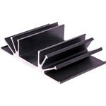
I saw a few digi-125 builds at the time PCBs were easy to buy. Directions for the amount of heatsinking were not covered in the article though, since the power rating was arbitrary - up to you with only suggestions for suitable power transistor types.
In the same spirit of cheapness, some constructors just bought short, packaged lengths of the extruded aluminium section, similar to that shown attached. These were likely bolted flat to the rear of a steel amplifier case and only just accommodated 2 x TO3 transistors, unsuitable for more than light duty. Yes, this did result in overheating as you might expect when run at party level and I believe that some amps were oscillating in that dire condition as they died.
A fire though, requires something combustible, not TO3 transistors but probably the plastic TO92 drivers, before they died trying to supply the current to sustain oscillation. This doesn't amount to a bad design but rather the article was pitched at constructors who already had some understanding of audio power amplifiers and their requirements for safety and cooling. I don't think that electronic hobby magazine readers in general, were so well informed.
Attachments
- Status
- This old topic is closed. If you want to reopen this topic, contact a moderator using the "Report Post" button.
- Home
- Amplifiers
- Solid State
- DIGI-125 Kit Amplifier Module