Yes, I have. I have four of the digi125 modules constructed 19 years ago "no mods" configured as bridged pairs (bridge mode)
using the MJ802/MJ4502 devices driving a pair of three way speakers "15 inch drivers".
I have never had a failure in the amp in all these years, the soundstage is just as open and crisp as the day I finished the project, sound pressure levels are impressive "that tight punch in the gut sort of thing".
It can handle anything from classical to rock and at full power there is no noticeable distortion at all, except whats added by the vibrations that shake the hell out of my walls .
.
You must insure that the thermal design is well thought out, my amp generates an enormous amount of heat which is extracted with a pair of 120mm PC cooling fans and a large tunnel heat sink.
People will give you a ton of highly technical reasons why this amp is not up to par, I disagree with this simply because it SOUNDS AMAZING, "and is that not what its all about", cost around $300.00, and has never failed me in 19 years, actually I am in the middle of replacing the foam surrounds on the 15 inch drivers which have been destroyed over many years of musical enjoyment "and a few parties"
using the MJ802/MJ4502 devices driving a pair of three way speakers "15 inch drivers".
I have never had a failure in the amp in all these years, the soundstage is just as open and crisp as the day I finished the project, sound pressure levels are impressive "that tight punch in the gut sort of thing".
It can handle anything from classical to rock and at full power there is no noticeable distortion at all, except whats added by the vibrations that shake the hell out of my walls
.You must insure that the thermal design is well thought out, my amp generates an enormous amount of heat which is extracted with a pair of 120mm PC cooling fans and a large tunnel heat sink.
People will give you a ton of highly technical reasons why this amp is not up to par, I disagree with this simply because it SOUNDS AMAZING, "and is that not what its all about", cost around $300.00, and has never failed me in 19 years, actually I am in the middle of replacing the foam surrounds on the 15 inch drivers which have been destroyed over many years of musical enjoyment "and a few parties"
Just thought I would mention, in the schematic for the Digi 125, "R2" should be 4k7.
Errm, This resistor value for r2 quoted above, was a typo in a set of written instructions
from Greyham Dicker, on modifying the curcuit for 200 watts into 2 ohms.
The correct value is indeed 47k.
Sincere appologies to all.
If anyone wants the details I can upload a scan.
it would be great if you could upload a schematic with the correction
-Dan
Schematic in post #58 is correct.
Here is the 200w version instructions, from Greyham Dicker.
=======================================================
The secret to modifying the digi-125 amplifier to
produce 200 watts RMS into 2 ohms lies in some basic
improvements to the thermal design of the module.
Normally to produce levels of this amount one would
expect to find two pairs of MJ15003/004 devices in the
output stage, the main reason being to ensure the 50A
(Safe Operating Area) of the output devices are not
exceeded. We are able to obtain 200 watts from a pair
of devices and still remain inside the 50A by using two
design techniques. (1) by using low power supply rails
with a low load impedance, (2) by using good design
practice with regard for the thermal consideration.
Instead of mounting the module to a small aluminium
bracket and then to the heat sink we now mount the PCB,
and output transistors directly to a heat sink, this
lowers the thermal resistance to air and improves the
heat sink efficiency. Thus enabling us to use only one
pair of output devices. A large heat sink with a low
thermal resistance such as a DSE-H3472 or a JAYCAR
MF-21-1F-75 with a thermal resistance to air of
.6 deg/c/watt is recommended.
The changes required are to insert a wire link in the
PCB in place of R7 and R8 (as the output devices are not
turned on i.e. they are in class B no quiescent current
flows. This also improves the damping factor (lowers the output
impedance of the output stage.).
Q6 is changed for a MJ15003 and Q7 for a MJ15004
R6 must be a proper ½ watt resistor.
For increased voltage gain (av=50 instead of av=20)
R4 can be reduced in value to 2K2.
In the schematic diagram Q4 should be a BC556 R3 and
R2 should be 4k7
=======================================================
And a schematic without any errors.
=======================================================
The secret to modifying the digi-125 amplifier to
produce 200 watts RMS into 2 ohms lies in some basic
improvements to the thermal design of the module.
Normally to produce levels of this amount one would
expect to find two pairs of MJ15003/004 devices in the
output stage, the main reason being to ensure the 50A
(Safe Operating Area) of the output devices are not
exceeded. We are able to obtain 200 watts from a pair
of devices and still remain inside the 50A by using two
design techniques. (1) by using low power supply rails
with a low load impedance, (2) by using good design
practice with regard for the thermal consideration.
Instead of mounting the module to a small aluminium
bracket and then to the heat sink we now mount the PCB,
and output transistors directly to a heat sink, this
lowers the thermal resistance to air and improves the
heat sink efficiency. Thus enabling us to use only one
pair of output devices. A large heat sink with a low
thermal resistance such as a DSE-H3472 or a JAYCAR
MF-21-1F-75 with a thermal resistance to air of
.6 deg/c/watt is recommended.
The changes required are to insert a wire link in the
PCB in place of R7 and R8 (as the output devices are not
turned on i.e. they are in class B no quiescent current
flows. This also improves the damping factor (lowers the output
impedance of the output stage.).
Q6 is changed for a MJ15003 and Q7 for a MJ15004
R6 must be a proper ½ watt resistor.
For increased voltage gain (av=50 instead of av=20)
R4 can be reduced in value to 2K2.
In the schematic diagram Q4 should be a BC556 R3 and
R2 should be 4k7
=======================================================
And a schematic without any errors.
An externally hosted image should be here but it was not working when we last tested it.
Last edited:
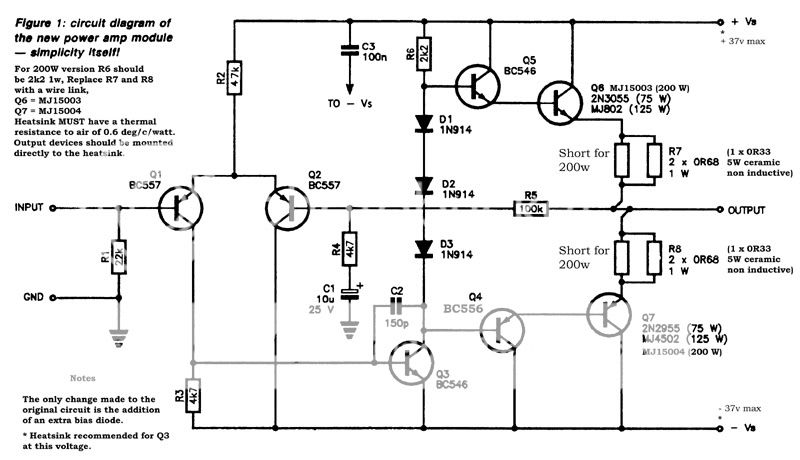
I made a couple of changes to the original circuit, split R6 into 820 (upper) and 1k2 (lower) resistors and put a bootstrap capacitor of 47uF between the junction and the output point - junction of R7 & 8. Also I joined the emitters of Q4 & Q5 with a resistor of 1K to assist the turn off of the output transistors.
Hi all,
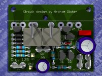
Just in case someone is interested, I have uploaded a PCB (and supporting files) for the DIGI-125 that I designed many years ago. I haven't actually made or tested the PCB but I have had a good success rate so far and wouldn't expect any major issues.
My thinking when designing this PCB was to remain "close" to the original schematic but make the PCB as small as possible, so the amp would compete with a gainclone type amps based on size and cost.
The zip file contains a schematic, a PCB etching file, a couple of stuffing guides, a BOM and a 3D picture.
regards
Attachments
.....isn't the input terminal a little close to the output?
Have you ever seen a chipamp? It's all relative.
Yes, you can - I used a similar design for my guitar amplifiers.
Use 100pF capacitor around VAS.
Use the THREE diode bias.
Use "Bone's" suggestion to split the 2K2 resistor to 1K2 and 820, along with 47uF bootstrap.
Use BD139 or similar for the VAS transistor - this does get HOT !!!
Use 0.47/5W emitter resistors for the TIP142/TIP147.
It will not be "hi-fi", but it actually sounds pretty good, better than LM3886.
Thanks for reply.. But i think I will go with SC5200 & SA1943.
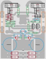
I have updated Greg Erskine's design for my need.
Thank you Greg Erskine sir for sharing the pcb Layout.
Please have a look and reply if you find any fault or suggestion.
Thanking
Rakesh Sharma
I have updated Greg Erskine's design for my need.
Thank you Greg Erskine sir for sharing the pcb Layout.
Please have a look and reply if you find any fault or suggestion.
Thanking
Rakesh Sharma
Attachments
Rakesh,
If you move your BD140 about 2mm to the left, you can then use a simple bended metal heatsink for both devices which will make them both more rigid and reduce any chance of touching each other..... use mica insulators on the devices, of course.
The angled piece need be no more than 1cms on each side, and 1cm deep.
Nice layout!
Hugh
Thanks AKSA Sir,
I have updated the PCB layout accordingly.
Just want to know that as i have changed BC546/557 to BD139/140, will this effects on the performance of this amp when used with 27-0-27 ac Transformer in powersupply.
Will BD139 on the extreme left also need Heat sink.
Thanking
Rakesh Sharma
I have updated the PCB layout accordingly.
Just want to know that as i have changed BC546/557 to BD139/140, will this effects on the performance of this amp when used with 27-0-27 ac Transformer in powersupply.
Will BD139 on the extreme left also need Heat sink.
Thanking
Rakesh Sharma
Attachments

Last edited:
- Status
- This old topic is closed. If you want to reopen this topic, contact a moderator using the "Report Post" button.
- Home
- Amplifiers
- Solid State
- DIGI-125 Kit Amplifier Module