Hi Chocolate, Sorry for the late reply was busy and learned how to draw using CAD software..
Here is the diagram. i actually attempted to draw it using CAD, i found a great tool called Eagle PCB, Eva used to draw her schematics.. rather easy to use as well")
Anyway here is a diagram note: The LM-311 Pins are wrong but you get the idea is a no brain er
Here is the diagram. i actually attempted to draw it using CAD, i found a great tool called Eagle PCB, Eva used to draw her schematics.. rather easy to use as well
Anyway here is a diagram note: The LM-311 Pins are wrong but you get the idea is a no brain er
An externally hosted image should be here but it was not working when we last tested it.
Last edited:
Hi All,
not to hijack the good thread, but then I didn't want to start a new one just for this.
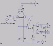
Working on a self-clocking board for the egan half-bridge module, I came up with this scheme to drive it.
Although phase is split twice, the idea is to keep timing under control. Due to Sunday brainfog , I'd appreciate comments. Notes:
- left out for clarity: feedback network, feedback for PS rejection, supply bypasses, current source and obviously the power module.
- Forget the ground symbol at VSS. System ground is mid-supply (VM).
- The LT1719 is real fast (4.5ns) and comes in a small sot23-6 package but I am thinking of a more standard package just to keep (slower) options open.
- the XOR split-and-deadtime circuitry is actually part of the egan module (it has a PWM input).
- The power module uses 5V for logic input and gate drive.
Thanks again
E
not to hijack the good thread, but then I didn't want to start a new one just for this.
Working on a self-clocking board for the egan half-bridge module, I came up with this scheme to drive it.
Although phase is split twice, the idea is to keep timing under control. Due to Sunday brainfog
, I'd appreciate comments. Notes:- left out for clarity: feedback network, feedback for PS rejection, supply bypasses, current source and obviously the power module.
- Forget the ground symbol at VSS. System ground is mid-supply (VM).
- The LT1719 is real fast (4.5ns) and comes in a small sot23-6 package but I am thinking of a more standard package just to keep (slower) options open.
- the XOR split-and-deadtime circuitry is actually part of the egan module (it has a PWM input).
- The power module uses 5V for logic input and gate drive.
Thanks again
E
Attachments
Firstly thanks Eva the probe tip helped alot waveforms looks more acceptable
Why didn't i think of that gizz the scope will of course introduce capacitive loading at the input... (Note the level shifting working with chocolate suggestion
Here are waveforms with the probe set to X1 (Note: Evident rise at foot of the wave (Ghost data that can make anyone read false diagnostics) )
Now the same waveform set to X10 (Wave looks acceptably good except for strange noise at the top (No ghost readings)
Next: Let me try chocolates suggestion regarding the level shift tweaks... (ill be back)
Why didn't i think of that gizz the scope will of course introduce capacitive loading at the input... (Note the level shifting working with chocolate suggestion
Here are waveforms with the probe set to X1 (Note: Evident rise at foot of the wave (Ghost data that can make anyone read false diagnostics) )
An externally hosted image should be here but it was not working when we last tested it.
Now the same waveform set to X10 (Wave looks acceptably good except for strange noise at the top (No ghost readings)
An externally hosted image should be here but it was not working when we last tested it.
Next: Let me try chocolates suggestion regarding the level shift tweaks... (ill be back
)In fact, there is redundancy overall: Compare; split and level-shift; re-compose a PWM; split again, and finally dead-time. I could put the comparator first, then level-downshift the PWM. But it would need two low-voltage rails around ground to feed the comparator... Other ways I tried (I know; I'm limited...I am not 100% convinced that you definitely need U7, except you have really small signals at the BJTs.
) to re-compose the PWM at the bottom of the differential pair invariably result in phase-asymmetry, hurting the output DC level which needs feedback to correct... Didn't like that.Well it's still developing, it uses EPC2001 eGaN FETs plus driver and DT control, all packaged in a 10-pin SIP module. Haven't updated its own thread in a while...What is the egan half-bridge module going to be?
How about...
R7 = 560
R8 = jumper
R9 = 1k2...1k5
Hi ChocoHolic
R7 = 680 (Didn't have a 560 at hand)
R8 = jumper
R9 = 1.5k + 1.5k = 3k
Level shift swings between 800mv (-Vcc) to 16V
Outputs from the CMOS XOR phase splitter, good looking waveforms with good asymmetrical split (no ugly artifacts)
An externally hosted image should be here but it was not working when we last tested it.
General Question:
What is the correct way to calculate: R7, R9 (I guessed the values 3k, this was dumb!.., i need the correct math to determine the correct values (This will of course be required when the power supply is increased higher than the current suppy (-21V/+21V), i selected values that saturated transistor)
Last edited:
I'm reconsidering the 250Khz clock, dropping it down to 150Kz no need to switch this fast considering its on a breadboard, and the more faster the modulator runs the more layout matters, and the more careful a designer should be.
I know EVA suggested some time ago doing Demo Class-D development requires new breadboards, rusty oxides contacts with old boards causes issues.
New bread board.
I know EVA suggested some time ago doing Demo Class-D development requires new breadboards, rusty oxides contacts with old boards causes issues.
New bread board.
An externally hosted image should be here but it was not working when we last tested it.
When this schematic is in working order and all power supply, noise immunity, EMI when the mosfets are introduced, has been taken care of i will start with house keeping.. some ideas i have.
PIC 1F628A Protection.
I liked the idea of introducing PIC based control / protection invitation, it really improves simplicity. Why do so many DIYers ignore the power of PIC based control systems for their amplifiers ?
PIC 1F628A Protection.
- Over Current.
- Over Voltage
- Under Voltage.
- Software Controlled Soft Start / Delay.
- Thermostatically controlled Fan.
- Maybe Last ERROR recall stored in the EPROM (am i pushing it )
I liked the idea of introducing PIC based control / protection invitation, it really improves simplicity. Why do so many DIYers ignore the power of PIC based control systems for their amplifiers ?
Last edited:
It's a question of experience, familiarity and mindset. When asked for a solution to a problem, one tends to use the tools one is most familiar with, regardless of objective fit.[...]Why do so many DIYers ignore the power of PIC based control systems for their amplifiers ?
Case in point, your own post!
: You prefix your ideas withPIC 1F628A Protection
That's putting the cart in front of the horse; instead of just stating "firmware", or "uC" you impose a specific architecture and a specific model right from the beginning. Presumably because you happen to be familiar with the PIC1F628A. By analogy, analog
DYIers (and the majority ef engineers) instinctively map a problem onto the set of tools and means they have experience with. While most of the time this turns out perfectly ok, sometimes the solution is convoluted, complicated and limited eg in expandability.Cheers,
E
I decided to use the LT1711 as one of my private standard comparators, because it appears to be an almost perfect comparator including the option to run the output stage at +/-5V.Try LT1711, nearly the same performance while it provides already symmetric outputs, perfectly time matched. BTW I'd be a bit affraid using a comparator that fast without any hysteresis whatsoever.
In the beginning I was also afraid to get 'ambitious output reactions' in applications without hysteresis, but even when running it on a bread board and using a noisy triangle it worked fine to generate pulses down to approx 10ns without uncontrolled panic at the output. Amazing device.
Please note the LT1719 does have a small hysteresis build in, could be the reason for elevator's choice.
P.S.
The package of the LT1711 is no fun on a breadboard....
P.P.S
My second standard comparator is the LM360.
I decided to use the LT1711 as one of my private standard comparators, because it appears to be an almost perfect comparator including the option to run the output stage at +/-5V.
In the beginning I was also afraid to get 'ambitious output reactions' in applications without hysteresis, but even when running it on a bread board and using a noisy triangle it worked fine to generate pulses down to approx 10ns without uncontrolled panic at the output. Amazing device.
Please note the LT1719 does have a small hysteresis build in, could be the reason for elevator's choice.
P.S.
The package of the LT1711 is no fun on a breadboard....
P.P.S
My second standard comparator is the LM360.
Hey choc the LM360 this is the cheapest comparator that offers complementary outputs
Guaranteed high speed: 20 ns max
... thanks for the heads up.
Last edited:
What is the correct way to calculate: R7, R9 (I guessed the values 3k, this was dumb!.., i need the correct math to determine the correct values (This will of course be required when the power supply is increased higher than the current suppy (-21V/+21V), i selected values that saturated transistor)
R7 defines the pull up current. A high pull up current is helpful to charge parasitic capacitances fast.
Ipullup=(5V-0.7V)/R7
But Ipullup must not be to high. First because it also pulls up the LOW level of the comparator output, which must be designed below 300mV. Otherwise LOW will not ensure to switch OFF the level shifter BJT properly. So for LM311 you should not go above 10mA. (If your real device on the desk has not read its data sheet, then already 10mA may cause LOW levels above 300mA Edit: 300mV . Did I hear 'fakes'? No, there are no fakes. But there are copies with a cost cut interpretation of the spec...)
The second reasond why Ipullup mustbnot be chosen extremely high, is that it also influences the losses in the level shifter transistor. P=Ipullup*Uce*DutyCycle
(Well these losses could be partially shifted into an additional series resistor, referring again to Nigel's posting).
R9 will be driven by the pull up current which was defined by R7.
Consequently the magnitude of the voltage across R9 will be U=R9*Ipullup.
Last edited:
Yeah, that small hysteresis sounded comforting[...] the LT1719 does have a small hysteresis build in, could be the reason for elevator's choice.
Since for this particular board, 5V is ok and complementary outputs are not needed, I'm also looking at the LMV7219 and the slower, pin-compatible LMV7239.Anyway, speaking of comparators and micros, years ago I was working on a project which used a Silicon Labs micro. Like most of their micros, it had a built-in comparator with software-settable response time (from ~100ns to ~1us) and hysteresis. So I thought about building a class-d amp based on such a microcontroller just for the fun of it. For example, it could generate PWM on its own (for test purposes, monitoring current consumption and heat sink temperature, adapting dead time via a digital pot), or monitor the PWM duty cycle to avoid overdrive by randomly sampling it etc. and the more the merrier but you get the idea
. Long story short I still have to build one, but promised, one of these weekends...
But take care. LM360 is not designed to run the output stage at +/-5V.
Go for LM361 which has same specs 20nS delay and complementary outputs but also works on +/-15V like an opamp frontend and +5V for logic interface
- Status
- This old topic is closed. If you want to reopen this topic, contact a moderator using the "Report Post" button.
- Home
- Amplifiers
- Class D
- Differential phase splitter with level shift capability