Hi,
if this amp is for high fidelity, then the DT is wrong. not only the time (60ns) you have to look at. but the point at which the transition occurs.
I see that this signal has a lot of distortion at low signal levels, and at high frequencies of the audio band. Also, turn-on MOSFET have very up delay. ..We believe that the MOSFET remains cold")
if this amp is for high fidelity, then the DT is wrong. not only the time (60ns) you have to look at. but the point at which the transition occurs.
I see that this signal has a lot of distortion at low signal levels, and at high frequencies of the audio band. Also, turn-on MOSFET have very up delay. ..We believe that the MOSFET remains cold
Hi,
if this amp is for high fidelity, then the DT is wrong. not only the time (60ns) you have to look at. but the point at which the transition occurs.
I see that this signal has a lot of distortion at low signal levels, and at high frequencies of the audio band. Also, turn-on MOSFET have very up delay. ..We believe that the MOSFET remains cold
The amp is planed for sub-woofer usage, if so whats wrong with 60ns even if it was planned for full range?
The amp is planed for sub-woofer usage, if so whats wrong with 60ns even if it was planned for full range?
Hi, time of dt is relative. (depeand a mode that use)
In your case (your dt on oscilloscope) is wrong,also it is responsible for some defects, including ringing you delete with RC (this is another mistake)
when adjust a class D amplifier, you must also consider aspects related to the sound. (not only if the pwm is clean).
This is one reason that many Class D amps, they sound so bad.
All know that is not simple, and all know that not exist a right science but only formulas by formulas
Attachments
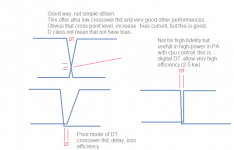
whats wrong with 60ns even if it was planned for full range?
Just search for dead time distortion.
But don't bother - you can adjust this in a later step.
It is not an urgent task to tune a car with a front spoiler, before the engine runs on all cylindres.
Furtheron your setting with long dead time and no filter, is systematically triggering resonances. Means, it magnifies ringing issues and by this is a good mode of operation to design reasonable snubbers.
Don't get tricked by the common approach, where people put the filter and then watch the signals during idle. That's the method to ensure running blind.... and then wonder about phantom shut downs at high ouput levels, or even suffer from 'absolutely unexplainable defects'...
At AP2:
Why do you generally reject snubbering?
Hi,
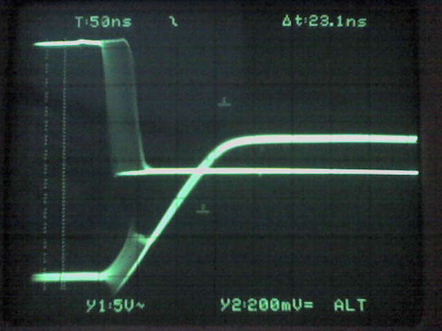
My ref is on N.4 scope of reactance (in dt 60nS), i suppose probe is at node pre-filter output. this figure i see not good for hi-fi amp.
independant if is better 100nS or 30nS, this is not 60nS real,(in fact mosfet remaining cool), because in the point of transition, Both MOSFETs have dead time. (then there is no bias current (open)). Of course this increases the crossover distortion and introduces other defects.
Also, ringing That you see (i see big), this is generated by the lack of load across the output.
i mean, the instant that the high-side switch off, the current flow (becouse node is open) tries to get back inverted phase. In fact, the amplitude of the ringing wave is very similar to "alpha", just the down side switch on.
To Reactance: Please, if you can modify dt (even you measure 50mA at 50V) then ,see ringing now.
In general, is correct a very low value of rc (if necessary) for eliminate very small ringing. as inductance of drain etc..
I mean in all..first, eliminate nature of defect. after try to tuned some thing.
Also, ringing That you see (i see big), this is generated by the lack of load across the output.
An inductive idling filter would hide the ringing issues, giving great screen shots to show around.
But as soon as you would run with signal and a load current that is larger than the filter ripple - the ringing will come up again.
You can cure the ringing by a RC-snubber or by a special choke, but you have to do something about it.
Hi,
My ref is on N.4 scope of reactance (in dt 60nS), i suppose probe is at node pre-filter output. this figure i see not good for hi-fi amp.
independant if is better 100nS or 30nS, this is not 60nS real,(in fact mosfet remaining cool), because in the point of transition, Both MOSFETs have dead time. (then there is no bias current (open)). Of course this increases the crossover distortion and introduces other defects.
Also, ringing That you see (i see big), this is generated by the lack of load across the output.
i mean, the instant that the high-side switch off, the current flow (becouse node is open) tries to get back inverted phase. In fact, the amplitude of the ringing wave is very similar to "alpha", just the down side switch on.
To Reactance: Please, if you can modify dt (even you measure 50mA at 50V) then ,see ringing now.
In general, is correct a very low value of rc (if necessary) for eliminate very small ringing. as inductance of drain etc..
I mean in all..first, eliminate nature of defect. after try to tuned some thing.
Looking at older reference designs from EVA, from notice the large amount of dead-time in this project as well however most importantly notice the smooth transitions during switching this is a combination of tight PCB layout, years of experience and tricks of the trade.
Ive actually reduced dead-time which used to sit at a ridiculous 100>ns, and reduced it to 60ns of deadtime, no cross conduction and shoot through.
was experienced.
Also note.. i haven't made ANY effort simulating parasitics introduced by the circuit (taken into account that its build on a breadboard running at a clock @ 250khz.
Ive also undocumented more interesting findings, when placing 100uf/50v filter cap paralleled with 100nf near the supply ringing was dramatically reduced, which lead less ringing and less snubbing losses.
I'm actually waiting for my local supply for a filter CORE something like this.
Again 60u 35 OD should be okay, im tempted to use a ATX filter core (of course this wont woke so the project is on hold for now)
HF-157060-2 Arnold Powder Core
Hi,
My pic, include two output driver signals.
If you develop high level pcb-strategy,good components,correct filter output (inductor type right is AMIDON eg, 106 or 102 etc..) and correct signal that driving mosfet..yes, as surprise you can see a ringing but very very small. then use snuber for delete it. my snuber in old project have 220pF/22R. this have sense for me.(it is a simple small "load" just in high spectrum.(this extra oscillation can be up to 10x of frequency) all circuit incluse RF transmitter need this.
well,now i have one question for Choco. independant of all on circuit of amplifier A-B-D class,what is the bias current into your D amp? with such control signals to get this current bias? please, show me on scope.
this help my explanation.
This is the "key" to everything. becouse, as I have a bias current, how do I get this? I'll choose the way, will have much significance on audio performance.
It suffices that some companies would show the driver signal instead of some measures on the audio.!
@ AP2,
my critical comments are because you tend throw around words, without specifiying what you are talking about.
In this thread Reactance showed Ugs and Uds of the lower switch.
You jumped in with Ugs of upper and Ugs of lower switch, but not telling this in your original posting or drawing.
It is impossible to understand your postings - except for readers with identical or superior knowledge.
Partially this might be an issue of language, but frankly speaking it is more a question of posting discipline and precision.
@ALL:
Of course it is good for THD to run without a real dead time and to allow short cross conduction peaks resulting in a certain average current consumption of the switching stage - called by you bias.
And of course my adjustment is similar as proposed by you.
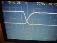
The first attached screen shot is showing Ugs of upper and Ugs of the lower MosFet. The probes were X10, means the vertical scale is 5V/grid. Time scale is 50ns/grid.
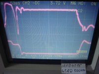
My snubbering of course is also smaller than described above, because I am adjusting the snubber geometry to use the parasitic snubber inductance and typically I get around with a snubber C of similar values like Coss, not 3 times of that. All the screen shots are done on a bread board with IRFB4115 snubbered with 500pF and 9.4 Ohms.
When running at approximately 400kHz and +/-60V rails, then the bias current of the switching stage is 110mA.
Different from Eva, I am not investigating all load situations in one modulated screen shot. I am forcing the power stage by DC load currents into any load situation that I desire to examine. Of course that's overtough for the entire power stage, but allows more precise examination. I do not have to make my living of that game, so I am not in a hurry and can play the slow game. Otherwise, 4 sure I would have to compress things like Eva does.
Forcing the power stage by DC currents is working like this:
-Putting a R L from output to pos or neg rail
-Adjusting the duty cycle to the desired value
By varying R and the duty cycle and chosing pos or neg rail you can get every load situation stationary and watch in very detail.
The second attached screen shot is done with 41A load from pos rail.
Operating frequency was close to 500kHz.
The upper trace shows Ugs of the lower Mos, 5V/Grid, 50ns/Grid.
The lower trace shows Uds of the lower Mos, 50V/Grid, 50ns/Grid.
P.S.
AP2, feel free to post the same signals including heavy load situation from a professional amp, instead from a bread board.
my critical comments are because you tend throw around words, without specifiying what you are talking about.
In this thread Reactance showed Ugs and Uds of the lower switch.
You jumped in with Ugs of upper and Ugs of lower switch, but not telling this in your original posting or drawing.
It is impossible to understand your postings - except for readers with identical or superior knowledge.
Partially this might be an issue of language, but frankly speaking it is more a question of posting discipline and precision.
@ALL:
Of course it is good for THD to run without a real dead time and to allow short cross conduction peaks resulting in a certain average current consumption of the switching stage - called by you bias.
And of course my adjustment is similar as proposed by you.
The first attached screen shot is showing Ugs of upper and Ugs of the lower MosFet. The probes were X10, means the vertical scale is 5V/grid. Time scale is 50ns/grid.
My snubbering of course is also smaller than described above, because I am adjusting the snubber geometry to use the parasitic snubber inductance and typically I get around with a snubber C of similar values like Coss, not 3 times of that. All the screen shots are done on a bread board with IRFB4115 snubbered with 500pF and 9.4 Ohms.
When running at approximately 400kHz and +/-60V rails, then the bias current of the switching stage is 110mA.
Different from Eva, I am not investigating all load situations in one modulated screen shot. I am forcing the power stage by DC load currents into any load situation that I desire to examine. Of course that's overtough for the entire power stage, but allows more precise examination. I do not have to make my living of that game, so I am not in a hurry and can play the slow game. Otherwise, 4 sure I would have to compress things like Eva does.
Forcing the power stage by DC currents is working like this:
-Putting a R L from output to pos or neg rail
-Adjusting the duty cycle to the desired value
By varying R and the duty cycle and chosing pos or neg rail you can get every load situation stationary and watch in very detail.
The second attached screen shot is done with 41A load from pos rail.
Operating frequency was close to 500kHz.
The upper trace shows Ugs of the lower Mos, 5V/Grid, 50ns/Grid.
The lower trace shows Uds of the lower Mos, 50V/Grid, 50ns/Grid.
P.S.
AP2, feel free to post the same signals including heavy load situation from a professional amp, instead from a bread board.
Attachments
Hi Choco
I jumped on the thread without understanding that the signal on the oscilloscope was referring to Ugs-Uds on lower switch. sorry for this too reactance also.
So some of my comments are worthless.
It was not my intention to criticize the work of reactance, but help him.
However, some things I said (as I see that you know well), many do not know them, and continue on the wrong path.
Unfortunately at this time, I can not put some photos of signs in different circumstances. (not for game)
A good class D amp, must have enough bias. (obvious that is obtained in a different way, from the class AB). but I call "bias" becouse it is bias. (quiescent current) and allowing more linearity in the transition, especially at low loads.
Usually speech, becouse class d has a major role in the PA, many think that is the same use in audiophile room.
No. There is a huge difference between the two uses, and many parameters up today are not perfect yet, some think they have solved, just because they have a lot of strange feedback circuitry to continuously adjust the phase loop and the other circuits to prevent its collapse when no load .. etc etc..
I respect EVA (although sometimes he attacks me) but I have no news that has made an amp with high resolution, so it can not be my reference.
I think you are on the good way for good amplifier.
Regards
Hi Choco
I jumped on the thread without understanding that the signal on the oscilloscope was referring to Ugs-Uds on lower switch. sorry for this too reactance also.
So some of my comments are worthless.
It was not my intention to criticize the work of reactance, but help him.
However, some things I said (as I see that you know well), many do not know them, and continue on the wrong path.
Unfortunately at this time, I can not put some photos of signs in different circumstances. (not for game)
A good class D amp, must have enough bias. (obvious that is obtained in a different way, from the class AB). but I call "bias" becouse it is bias. (quiescent current) and allowing more linearity in the transition, especially at low loads.
Usually speech, becouse class d has a major role in the PA, many think that is the same use in audiophile room.
No. There is a huge difference between the two uses, and many parameters up today are not perfect yet, some think they have solved, just because they have a lot of strange feedback circuitry to continuously adjust the phase loop and the other circuits to prevent its collapse when no load .. etc etc..
I respect EVA (although sometimes he attacks me) but I have no news that has made an amp with high resolution, so it can not be my reference.
I think you are on the good way for good amplifier.
Regards
All i wanted to build is great sounding class d amplifier for a sub-woofer DIY style, hands dirty
with care of course that's why i used a +/- 21volt supply(taking into account its my first experience constructing one)Really i dont think you should go on a "trip" expressing your dislike and use big words and terminology that a only few understand.. Eva does the same but the up side is she has a way more experience and wisdom then most of the people here as she makes a living out of this stuff, i used her designs as a guideline (even though its old) however its exactly what i was look in a design guide, evidence (proof of concept) including PCB layouts.. maybe if you did the same by extending your tips with "real" evidence i would understand you but i don't so i cant put together a thing you say.
Example: Look at the tip i got from her, implementing "DSP IIR filter" DC detection using a 8-bit micro-controller, i don't think anyone here has ever gone that far and if they did again where is the evidence? too much big talk no evidence.
(and it's not the first time she mentioned PIC based control circuity)
Look im just a newbie and im putting together the tips and tricks everyone here has generously offered me, most importantly chocolates helped me a lot.
And oh she attacks anyone that doesn't make sense.. shes tired on hearing the same dumb questions over and over again (5 years ago she was way more helpful i can tell by the amount of stuff posted) and most of the stuff i found dates back 5 years ago and even today in 2012 people are still asking stupid questions.. that's why i didn't post any questions (yet) about output filters cause its been discussed over rand over again. and i look a dated stuff that still have relevance.
Last edited:
@AP2:
...hope I was not to unfriendly... trying to push you to generate more understandable posts.
Regarding being on the right way for a good amp:
After a more detailed analysis of the noise and jitter mechanism of my PWM, I decided to redesign my modulator...
DIY is great. You can design for performance instead for lowest cost and shortest time to market.
@Reactance:
Dead time distortion is a valid concern. And dead time distortion can be unpleasant also in a sub. Some subs have the unpleasant nature to show low efficiency at the frequency that they shall reproduce, but high efficiency at typical spectrum of dead time distortion. Especially critical are small designs which use the linkwitz transform for correction.
As soon as your snubbers do satisfy you, it is starting to make sense to reduce the dead time.
Most simple method for a reasonable dead time setting:
- Have the output filter connected.
- Step down the dead time and watch the current consumption. There will be a point where already small steps will cause a remarkable increase of the current consumption. Here cross conduction peaks are starting. Fine tune dead time to a level which results in approx 10°C temp rise of the heat sink during idle with filter connected. Unexpected but true - I never observed a tendency of thermal runaway in such class D half bridges.
When adjusted like this (or even higher) it always was a pretty stable thing.
You can test it by heating up the heat sink to 80°C by a hair dryer. After stopping the hair dryer the system should cool down again to the level before being heated up by the hair dryer.
@AP2:
...hope I was not to unfriendly... trying to push you to generate more understandable posts.
Regarding being on the right way for a good amp:
After a more detailed analysis of the noise and jitter mechanism of my PWM, I decided to redesign my modulator...
DIY is great. You can design for performance instead for lowest cost and shortest time to market.
@Reactance:
Dead time distortion is a valid concern. And dead time distortion can be unpleasant also in a sub. Some subs have the unpleasant nature to show low efficiency at the frequency that they shall reproduce, but high efficiency at typical spectrum of dead time distortion. Especially critical are small designs which use the linkwitz transform for correction.
As soon as your snubbers do satisfy you, it is starting to make sense to reduce the dead time.
Most simple method for a reasonable dead time setting:
- Have the output filter connected.
- Step down the dead time and watch the current consumption. There will be a point where already small steps will cause a remarkable increase of the current consumption. Here cross conduction peaks are starting. Fine tune dead time to a level which results in approx 10°C temp rise of the heat sink during idle with filter connected. Unexpected but true - I never observed a tendency of thermal runaway in such class D half bridges.
When adjusted like this (or even higher) it always was a pretty stable thing.
You can test it by heating up the heat sink to 80°C by a hair dryer. After stopping the hair dryer the system should cool down again to the level before being heated up by the hair dryer.
@AP2 and @Choc
Point taken guys, dead time is critical interns of sound quality THD, i will experiment with this later their is still much to do.
Lost interest?
Design already sold?
Tutor/Prof satisfied?
Got Married, project is on hold, not for sale, i dont make proft with electronics i write software for a living.
- Status
- This old topic is closed. If you want to reopen this topic, contact a moderator using the "Report Post" button.
- Home
- Amplifiers
- Class D
- Differential phase splitter with level shift capability