Thanks, continuing to look at your web page, and return to the thread.
http://www.linear.com/company/software.jsp
http://www.linear.com/company/software.jsp
Well... I am afraid that I cannot contribute very much here.
I am a class D Rookie (should I also name my sub amp this way? )
)
Somebody told me about dead time distorsion, then I read one thread here and for me that was enough. It is basically fitting to my imagination that dead times may cause distorsion, depending on the load and signal. As per my understanding the reason for this is the hard-to-predict output voltage of the half bridge during the dead time. It is also obvious for me that high AC ripple in the output filter is helpfull to fight the dead time distorsions. If the ripple is high, then during the dead time the inductive energy of the filter choke will immediately push the halfbridge ouptut to the opposite rail as soon as we open one switch and the current will run through the freewheeling diode until the related switch will be turned on. So the output voltage of the half bridge is almost always defined by upper or lower rail.
This condition is valid only as long as the HF current ripple peak is with some margin higher than the output current (required margin depends of course on the dead time).
Important for me was the information that the dead time distorsions have a similar spectrum as the cross over distorsions in class B designs. I already experienced that my ears are sensitive on this.
Ok, I didn't need to know more... things are making basically sense to me... and consequently I am putting some weight to optimize the dead time in my design...
My switching frequency will be around 100kHz. My dead time adjustment now is close to cross conduction, something between zero and 10ns. Also it seems to be quite stable vs. temperature and load. Not completely independend, but amazing stable!
My output inductors are two 45uH beasts (full bridge with +/-55V) and the resulting ripple current is about +/-3A peak.
Up to now that's 100% of my dead time distorsion know how.
I am a class D Rookie (should I also name my sub amp this way?
)Somebody told me about dead time distorsion, then I read one thread here and for me that was enough. It is basically fitting to my imagination that dead times may cause distorsion, depending on the load and signal. As per my understanding the reason for this is the hard-to-predict output voltage of the half bridge during the dead time. It is also obvious for me that high AC ripple in the output filter is helpfull to fight the dead time distorsions. If the ripple is high, then during the dead time the inductive energy of the filter choke will immediately push the halfbridge ouptut to the opposite rail as soon as we open one switch and the current will run through the freewheeling diode until the related switch will be turned on. So the output voltage of the half bridge is almost always defined by upper or lower rail.
This condition is valid only as long as the HF current ripple peak is with some margin higher than the output current (required margin depends of course on the dead time).
Important for me was the information that the dead time distorsions have a similar spectrum as the cross over distorsions in class B designs. I already experienced that my ears are sensitive on this.
Ok, I didn't need to know more... things are making basically sense to me... and consequently I am putting some weight to optimize the dead time in my design...
My switching frequency will be around 100kHz. My dead time adjustment now is close to cross conduction, something between zero and 10ns. Also it seems to be quite stable vs. temperature and load. Not completely independend, but amazing stable!
My output inductors are two 45uH beasts (full bridge with +/-55V) and the resulting ripple current is about +/-3A peak.
Up to now that's 100% of my dead time distorsion know how.
my understanding of dead time is even simpler than ChocoHolic's!
dead time is the delay between the input turns on and the output turns on. a pwm amplifier is essentially switching the output to either the positive rail and the negative rail. To output very small voltages, the switching has to be done very very fast / frequent.
Well, if the dead time is too long, the output will be stuck with either rail longer than needed and the amp wouldn't be able to reproduce small voltage output.
It seems to me that there is some compromise between cross conduction and dead time. I think that with faster slew rate one can have resonably low conduction and dead time, but high slew may require a more sophisticated mosfet driver with higher current abilities.
Just thoughts from a guy, who thinks ChocoHolic the 'rookie' is a true expert. I suspect I am not alone with this opinion
regards
Adam
Just thoughts from a guy, who thinks ChocoHolic the 'rookie' is a true expert. I suspect I am not alone with this opinion
regards
Adam
Fokker isn't quite right. Dead time is the time allowed in the driver stage between turning one FET off, and turning the other side FET on. If the top FET (for example) isn't fully turned off before the bottom FET turns on, then you'll have a big spike of wasted current flowing all the way between the +ve rail and the -ve rail, not going via the wanted path through the output filter coil.
If the dead time is too long though, you'll have a period where neither FET is on, resulting (especially in open-loop amplifiers) in a period where you are not in control of the output, very much like you get around 0V in an under-biased class-B amp.
If the dead time is too long though, you'll have a period where neither FET is on, resulting (especially in open-loop amplifiers) in a period where you are not in control of the output, very much like you get around 0V in an under-biased class-B amp.
There are technical similarities between classB distortion and dead time classD distortion, but in classD when input signal goes higher level, THD goes up too.
Another words distortion vs. level is monotonically rising function, which is desirable in my opinion and in opinion of for example N. Pass as far as I remember.
This is 'natural' distortion mechanism, similarly speakers distort monotinally, so classD designs don't really need so low THD numbers as class(A)B.
regards
Adam
Ouroboros said:If the dead time is too long though, you'll have a period where neither FET is on, resulting (especially in open-loop amplifiers) in a period where you are not in control of the output, very much like you get around 0V in an under-biased class-B amp. [/B]
I often need to run Class B with very low quiescent currents, and usually end up under biasing. In these applications, 10% THD is quite aceptable (could be higher, but not desireable!)
According to the Philips notes that accompany their UcD demonstration PCB, it is a simple job to adjust the dead time by changing the value of one resistor.
It'll be interesting to see just how much quiescent current can be reduced by running a UcD amp with a THD of 10%. Hopefully, quite a significant amount!
poobah said:Guys.
These half bridges drive an inductor... right? When the top transistor turns off... and the bottom transistor is not yet on... where does the inductor get its current? (another reason why FETs are the preferred device).
It's probably a better reason for ZVS or ZCS.
According to the Philips notes that accompany their UcD demonstration PCB, it is a simple job to adjust the dead time by changing the value of one resistor.
Don't be letting that "app note" fool ya, that's only a means of dead time adjustment in the weakest possible sense.
rogs,
Don't count it... The dead time is a "guard band" value that has been chosen to avoid shoot-thru under any circumstances caused by component drift and production variations. The issue of shoot-thru certainly affects efficiency, but the design constraint is about keeping the FETs alive. So, you will probably not see any reduction in Iq by increasing the deadtime.
Don't count it... The dead time is a "guard band" value that has been chosen to avoid shoot-thru under any circumstances caused by component drift and production variations. The issue of shoot-thru certainly affects efficiency, but the design constraint is about keeping the FETs alive. So, you will probably not see any reduction in Iq by increasing the deadtime.
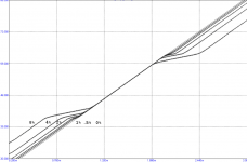
Guys, maybe i'm too late, but this is simple simulation can help figure out, how PWM linearity depends from the dead time (8,4,2,1,.5,0% of Tswitch). Easy to see, that the process haven't frequency dependance, so 100hz, 1khz or 10khz is no matter. BTW, several watts power region will have no dead time dependance also -only much more power level shows real THD, in other words, if your home cooked class D amp gave .002% at 1W, try to check it for 1/2 max power first.
Attachments
rogs said:According to the Philips notes that accompany their UcD demonstration PCB, it is a simple job to adjust the dead time by changing the value of one resistor.
that is particular to the design: a smaller resistor there will cause the current in the two driver transistors to reach its trigger levels faster on the lending edge / slower on the falling edge, thus reducing dead time.
The risk with that approach is that the amp may stop oscillating (too small of a resistor), or end up sticking to one rail (too high of a resistor).
As to distortion: well, human ears aren't that sensitive to distortion, especially with test tones. I played some test tones (sine, square and triangle) on my fucgger (that is outputing only the negative half so far) and my wife / kids couldn't tell them apart from the full wave version. It is easier with music but even that I would be surprised if anyone can tell thd within 10% in a dbt.
classd4sure said:Don't be letting that "app note" fool ya, that's only a means of dead time adjustment in the weakest possible sense.
I can confirm that the application note is right on that particular point. with a smaller resistor, it turns on the two coupling transistors (the ones that mate the differential comparators to the hi/lo-side drivers) faster.
It does change dead time in my fucgger implementation: the average current goes through the current limiting resistors goes up with smaller resistor but the change is quite dramatic so you will need to be careful playing with it.
If your driver has deadtime adjustment, I would use a lower resistor and let the driver handle the deadtime. if your driver does not have overshoot control (like the Maxim driver ICs with independent hi/lo side drivers), you can use that little resistor for dead time control.
What I am beginning to appreciate is that it is a mistake to try and equate D class 'deadtime' with B class 'under bias', when trying to vary quiescent current changes.
A B class amp running with no input signal, and no (or virtually no) bias will draw no current from the output stage -- both transistors are well and truly turned off - just a minimal current drain from any residual DC offset.
In the case of a similar state with no input signal, and an 'under biased' (excessive dead time) output , the class 'D' amp will still need to provide some current, even though its only overcoming switching losses, and ripple current sink/ source state changes, and this is likely to be significantly greater than the "equivalent" class 'B' current.
Hence the option to turn off the UcD -- it's a worthwhile saving!
Unfortunately I do not have that option in my application -I am required to run the amplifier(s) from battery power, and in an 'on' state, to allow fault monitoring.
And this is for 24 hours, at the end of which the amplifier has to provide full power for further 30 minutes!
All part of the specifications for emergency voice alarm systems.
So you'll understand the need for low quiescent current --to avoid having to use batteries the size of Belgium!
Excellent food for thought from the contributions here -- thanks guys!
So, how do you think it manages to effect the dead time?
Does it delay the rising edge, speed the falling edge, does it provide independant control of either slew rate or delay of either edge or both?
Is there anything else affected by the adjustment of it?
You'd really put your faith in a non intelligent gate driver, that's not even device and barely application specific? That'd be crude I think.
Right off the top of my head there's five other ways of affecting "deadtime" in that circuit that don't envolve the adjustment of that one resistor.
Its only use is as a "fine tune" and nothing more.
Cheers,
Chris
rogs said:What I am beginning to appreciate is that it is a mistake to try and equate D class 'deadtime' with B class 'under bias', when trying to vary quiescent current changes.
A B class amp running with no input signal, and no (or virtually no) bias will draw no current from the output stage -- both transistors are well and truly turned off - just a minimal current drain from any residual DC offset.
In the case of a similar state with no input signal, and an 'under biased' (excessive dead time) output , the class 'D' amp will still need to provide some current, even though its only overcoming switching losses, and ripple current sink/ source state changes, and this is likely to be significantly greater than the "equivalent" class 'B' current.
Hence the option to turn off the UcD -- it's a worthwhile saving!
Unfortunately I do not have that option in my application -I am required to run the amplifier(s) from battery power, and in an 'on' state, to allow fault monitoring.
And this is for 24 hours, at the end of which the amplifier has to provide full power for further 30 minutes!
All part of the specifications for emergency voice alarm systems.
So you'll understand the need for low quiescent current --to avoid having to use batteries the size of Belgium!
Excellent food for thought from the contributions here -- thanks guys!
Do whatever monitoring is required with micropower and have the output stage disabled when not needed. If you have to monitor the health of that as well, wake it up for a split second, then shut it off again. I don't see the sense in keeping it oscillating for nothing when you're on battery power with an emergency system. Also if the output stage is high impedance in a disabled state, you know it's OK.
Full power for 30 minutes should be no problem at all if designed properly.
During the dead-time, the inductor derives its voltage from the diode/switch on the rail opposite the one that was just turned on (active). The distortion comes from the fact that the other rail voltage has a diode drop added to it. This deviates from the expectation that the rails will be symmetric. This distortion falls with rising rail voltage as the diode drop looks smaller in comparison. All this ignores the on-state voltage drop of the switches.
Fet based designs, where the freewheeling is accomplished by a synchronous FET rather than an antiparallel or body diode minimize all this by virtue of the low conduction drop.
Remember, a MOSFET in the on state is happy to conduct in EITHER direction... this is the beauty thing about FET Class D and synch. rectification in general.
If you are talking about UPS duty here... most are thrilled silly with 5% THD. 10% is really the borderline if you want to say "TRUE SINE".
classd4sure said:So, how do you think it manages to effect the dead time?
Does it delay the rising edge, speed the falling edge, does it provide independant control of either slew rate or delay of either edge or both?
it controls the rising and falling edges. no it does not provide independant control, nor did Phillipse say it does.
classd4sure said:You'd really put your faith in a non intelligent gate driver, that's not even device and barely application specific? That'd be crude I think.
Well, we don't have device or application transistors, capacitor or resistors, for that matter. and we certainly don't have application-specific electrons. Any of the devices we use are not intelligent nor application specific at a level.
and there is no reason to have that application specific device.
fokker said:
it controls the rising and falling edges. no it does not provide independant control, nor did Phillipse say it does.
Well, we don't have device or application transistors, capacitor or resistors, for that matter. and we certainly don't have application electrons. Any of the devices we use are not intelligent nor application specific at a level.
and there is no reason to have that application specific device.
It controls the level of current output to the gate drivers. If you use an IC driver with a fet based input you're going to see a whole different story. That's all it does wrt deadtime.
We sure as hell do have application specific devices, your driver that "controls deadtime" is exactly that, and it'd be a rare occasion indeed where it would be up to the task of deadtime control all on its own.
So aside from that there's no application specific devices in electronics hmm... funny

- Status
- This old topic is closed. If you want to reopen this topic, contact a moderator using the "Report Post" button.
- Home
- Amplifiers
- Class D
- dead time, and class D distortion