If you want to make numerical comparison, you cant avoid defining in what space do you modell the network. Time? Frequency? Complex frequency? In time-domain and with generic waveform any relation is possible in specific moments. No way you can simply compare back EMF and applied voltage, ratio varies from -infinity to +infinity with time even with a simple sinus excitation.
In frequency domain it's advisable to specify what the assumed excitation signal is like (typically sinus) and how signals are represented (axsin+bxcos, or amplitude and phase, etc...).
Your first statement is true if you are talking about single frequency and effective values. But in this case there is no exception, back EMF will always be lower than excitation voltage, unless you make the speaker move from outside. But back EMF can be close in amplitude to the applied voltage and can have a significant phase-shift, so if you look at it in time domain, it can be reversed for a certain duration twice in every period. This is why a ClassAB amp must have a short circuit limit current much higher than 0, tipically 25...50% of max. current.
Summary: assumption of nonlinearity is not necessary to explain the exception in time domain, and not enough in case of frequency domain, unless you are talking about generation of harmonics, but this is simply the well known distortion, i dont think really related to this topic.
My comments are informed by real world experiences and observations, and confirmed by theory. This stuff actually happens in the real world and it can be duplicated on the bench whenever one decides to do the work.
For example this statement appears to be very general:
"But in this case there is no exception, back EMF will always be lower than excitation voltage, unless you make the speaker move from outside."
In the case of real world speaker drivers mounted inside real world enclosures, there is the slight matter of the air inside the enclosure.
Over a longer period of time the law of conservation of energy has to apply, but from instant to instant, not so much. Energy can be stored and released inside the system. The air can be a force that quite clearly makes the speaker cone move from a source that is outside of the speaker driver.
Therefore, the statement is true, but in the real world it does not explain away the role of nonlinearity in speaker driver motor assemblies.
And that my friend is why theory needs to be informed by practice. Theory may be 100% true as far as it goes, but there may be other stuff that is going on in the UUT that is before you.
Last edited:
Great discussion... did anyone bother about the definition of DF yet?
Post 75 - http://www.diyaudio.com/forums/solid-state/287072-damping-factor-explained-not-8.html#post4622558
Nice. Did you get a chance to use the resistor in the origional intent?Demo of damping using jneutron's super duper current sense resistor.
I took a biga$$ 12" woofer and carefully placed the tip of my Wiha screwdriver on the center of the dust cap and pulled it off as fast as possible to create a roughly equal relaxation from a fixed displacement under two conditions.
First I sensed the current with a .1 Ohm (jn is that what you sent me?) and gain of 90 voltage amplifier. The .1 Ohm shorts the speaker. In the second it is just the open-loop voltage. The damping should be obvious. Sometimes a simple visual display of what is going on physically is useful.
I've only made two values of these resistors, 100 milliohms and 1 ohm. I do not recall what I sent you. Count the total, N total resistors, R single value, total value=(4*R)/N.
A question. The first pic has a band around the value, is that amp noise at 50mV p-p? Edit: I erred, your using the amp as gain for the signal, not out to load as I first thought..
Is your amp doodling, humming to itself with noise until it is required to do something, and then quiets down and gets to work? Perhaps tossing a small amount of quite DC into the amp will show if there is voltage dependent noise being generated..
I remember an old aaron gavin eq I built from kit, it would breath when signal was present, generating hiss modulated by a 20 hz high amplitude sine.
John
Last edited:
I stand corrected....
Thanks for the suggestions. I've also discussed that problem with co-workers. Another variant in the resistor is to keep each direction isolated and use 4 plates. I did this for my EDM setup where I wanted to view the current of the spark at nanosecond levels, and needed a load resistor in series to control the spark maximum current. My first pass uses a .05 ohm CVR with a 10 ohm interleaved resistor. The coax turned into a half inch wide copper braid pair separated by a .5 mil layer of kapton (with glue, 1.5 mil total) for a characteristic impedance close to load resistance., and short, very short.Thanks! This (through hole 3D layout) is a new approach for me, I was thinking in 2 layer SMD. Still have to figure out in what path to connect it to avoid transinductance between current to be measured and sensed voltage. External inductance is also a problem at 1 mOhm, only 2...5 nH is tolerable for me...
Suggestion for terminology: you could think this network as a transimpedance with 2 ports (however on your picture these ports are not defined, but the usage is this). Instead of external and internal inductance you can say input- and trans-inductance (and -resistance). This describes the important behaviour well, and nobody will ask you where is inside and outside.
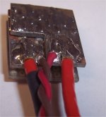
I've attached another pic of a CVR I made. Current is the two outer untwisted 12 gauge wires, v tap is the center twisted pair (to remove coupling to current in the wires. I also made a few where the current enters coaxially, braid to first surface, core enters through hole.
I've been considering how to do it with surface mount. Most of my thinking unfortunately results in a 3D structure, and requires a step soldering process using tin/silver eutectic first and then tin/lead eutectic for final assembly. Unfortunately, 215 C vapor phase reflow flourinert is waaaay too expensive for my personal use. edit: trying to do it 2-d ends up with significant board area with prop delays due to physical size. Not an issue at audio of course, but I tend towards "slight" overkill, like 5 or 6 orders of magnitude where possible...
John
Attachments
Last edited:
Summary: assumption of nonlinearity is not neccessary to explain the exception in time domain, and not enough in case of frequency domain, unless you are talking about generation of harmonics, but this is simply the well known distortion, i dont think really related to this topic.
Pafi,
You are quite accurate in your understandings and statements.
John
Scott: I messed up the post during edit...meant to say.. It looks like your noise reduces significantly when the voltage slews. It's a bit difficult to see well as it would be a vertical 50mV superimposed on the high slew.
Last edited:
Nice. Did you get a chance to use the resistor in the origional intent?
Still on my to do list, I've been packed and ready for a move for more than a month. There is a feature in the Analog Discovery where it shows the extent of noise before decimation since it digitizes at max rate.
Still on my to do list, I've been packed and ready for a move for more than a month. There is a feature in the Analog Discovery where it shows the extent of noise before decimation since it digitizes at max rate.
Does it mention lowering of noise during signal slew?
John
Does it mention lowering of noise during signal slew?
John
Not directly, I think it just decimates down to a lower effective sampling rate.
Pafi,
Don't forget, the massive anti-parallel structure also increases distributed capacitance if you're looking at very high frequency use. Since the current interleaves within a structure that supports voltage gradients, the capacitance will not follow the typical LC=1034 DC equation. The common side has no voltage, and it gradients across the resistor lengths. I suspect the capacitance will scale as 1/2 times 1/sqr(2), or .7071 divided by 2. Roughly 1/3rd of T-line value.
I would use an effective permittivity of 5 as a guess, plug in to calcu C from a transmission line, then take 1/3rd of it..
LC = 1034 DC, L in nH per foot, C in pF per foot.
Structure inductance, use 200 nH per foot, then divide by the number of pairs of resistors being used. Then take about 2% of that per foot value (resistor length of .25 inch divided by 12 inches).
John
edit: Oh sorry, DC is relative permittivity, not free space.
Last edited:
jneutron!
Thank you for the ideas, but in my project the whole loop inductance (voltage source + current controller + sense resistor + load) must be under 3...5 nH, not only transfer inductance is important, and this 3D arrangement is not easy to connect with really low input inductance, so I stay with the original plan (current flows in and out on 2 different, wide layers of a thin PCB in opposite directions) with some modification (many little resistors instead of 1 resistive plane). The output will be routed in a way flux should induce close to zero voltage in it. (Much less than 1 mm^2 loop area close to flowing current which is distributed to 10 paths.) I will flip SM resistors to make current flow closer to the ground plane and sensing tracks also. This way not only transfer inductance can be held well under 0.1 nH, but input inductance will also be less than 0.3 nH.
(+The complete structure will be mirrored to the other side of the GND plane also...)
Capacitance is perfectly negligible, since impedances are veeery low. I need only 2...5 MHz cutoff frequency in the control loop.
Yes, of course, I meant that but you worded it better than meStrictly speaking a short cannot absorb any energy. However, it allows the resistance in the circuit (mainly voice coil, plus cables and crossover) to absorb the energy by maximising the current.
What are the effects of back EMF on digital amplifiers ?
Regards.
You mean class D probably. Same thing. Take a black box with a class (A)B amp or a class D amp inside, from the outside the speaker just sees a very low internal impedance. Doesn't matter how it is created.
Jan
Pafi:
Great, sounds good.
Be careful however with soldering surface mount resistors upside down. The black overcoat is there to protect the resistive element from solder. If it is mis-registered a bit and does not extend over the endcap metallization, the solder can leach out the resistive material, and the resistor can fail right away, or in a little time. If you lose even one in a massively parallel construct, the inductive cancellation will be totaled.
If you examine the top very carefully, look for exposed alumina on the edge, the ends will look like "T" shape if it's compromised.
John
Last edited:
Jan,
When do you leave on your trip? I have some drawings explaining the VI ellipse, and how to get a secondary locked signal to exercise the limits of the VI space.
It will go a long way towards explaining why a 3 way system can exert 1/3rd of it's nominal impedance to the amp, causing current clamping if the amp doesn't have the headroom in the drive.
Also, it shows how the damping factor can be tested in each quadrant.
I can put it up monday late in the day. EST of course..
John
@JN:
John now that you are here I have a somewhat off-topic question (but it's my thread so there!):
I am studying SOA-related stuff. One app note discusses the impact of pulse duration on the allowable SOA - SOA graphs normally give different curves for different pulse duration. So far so good.
Then they say, if you have longer/more pulses adjust it (they give a formula) according to the adjusted Ztjc.
And indeed, the data sheet has a graph of Ztjc versus pulse duration. What I do not understand is why Ztjc would be dependent of pulse duration - isn't Ztjc a property of the physical device, die, case? How can an 'impedance' change with pulse duration?
As compensation for your thinking, see attached which is probably of interest to you.
Jan
John now that you are here
I have a somewhat off-topic question (but it's my thread so there!):I am studying SOA-related stuff. One app note discusses the impact of pulse duration on the allowable SOA - SOA graphs normally give different curves for different pulse duration. So far so good.
Then they say, if you have longer/more pulses adjust it (they give a formula) according to the adjusted Ztjc.
And indeed, the data sheet has a graph of Ztjc versus pulse duration. What I do not understand is why Ztjc would be dependent of pulse duration - isn't Ztjc a property of the physical device, die, case? How can an 'impedance' change with pulse duration?
As compensation for your thinking, see attached which is probably of interest to you.
Jan
Attachments
Ztjc is an approximation of a 3d thermal path with different conductivities and heat capacity
simpler but still useful than a single number is a 2d model, a string of thermal resistances with heat capacity "capacitors", a few nodes may just be the chip, the bonding, the package metal, the gap filler, the external heatsink
the thermal analogy capacitances representing heat capacity are all "grounded", it takes watts x time to "charge" the heat capacity to a temperature (rise)
the longer the pulse the more of the more distant thermal path, heat capacities come into play, the more a single Ztjc number has to be changed to give a reasonable approximation
jcx has it spot on. They are relying on the heat capacity to support the higher dissipation with shorter pulses. For example, IRfets diffused structure and topology is capable of much more stable dissipation than the physical structure is capable of transferring out of the junction. As switchmode applications gained traction, IR used this fact to allow designers to get significantly more use out of a specific die, whereas normal bipolars would jump into secondary breakdown if they were worked that hard, and might not recover in time for the next pulse... So they really had to explain to the designers how this actually worked, and how it was so much different than bipolars.@JN:
John now that you are here
I am studying SOA-related stuff. One app note discusses the impact of pulse duration on the allowable SOA - SOA graphs normally give different curves for different pulse duration. So far so good.
Then they say, if you have longer/more pulses adjust it (they give a formula) according to the adjusted Ztjc.
And indeed, the data sheet has a graph of Ztjc versus pulse duration. What I do not understand is why Ztjc would be dependent of pulse duration - isn't Ztjc a property of the physical device, die, case? How can an 'impedance' change with pulse duration?
As compensation for your thinking, see attached which is probably of interest to you.
Jan
Their explanations really were not that good, but hey, so far it's worked..it was a marketing tool for the product line.
Thanks for the article. That circuit topology is exactly what Lorlin(now Eaton I think) used in their semiconductor test systems, an Impact II test system was what I used back in '82. BVcer(sus) used the common base configuration, ramped the collector voltage to setpoint, pushed the emitter current, then made a pass/fail decision based on the emitter to ground voltage.
This particular test method also exercises the uniformity of the C-B diffusion profile under the emitter fingers, a problem I never found in the industry literature but had to figure out myself.. When the CB voltage is setup, the unused CB diffusion (what's left before CB breakdown) gives higher gain to the device, and if the CB junction is not uniform enough, the device will go secondary at the thin spots during the current slew, and it melts the silicon in that spot. The failure spot will be extremely difficult to find if the metalization is thick, but it can be found under a metallurgical with polarization. Devices which will fail this way can be found with a punch-through test. In fact, since my employer was pushing many devices, especially new generation hv/fast/rf devices, it became necessary to use a punch through test to be sure they were not designing in problems. If the hybrid circuit used too high a voltage and slewed it from zero current to max too fast, we had to make sure devices which exhibited punch through were not selected for the build run. The Impact allowed automatic comparison between BVcbo and BVces.
The setup you provided will spot those devices, although I suspect they did not realize it. They were only interested in production, and had a basic interest in the die attach integrity. When I get the chance, I'll comb through the entire article.
Thanks, John
Last edited:
- Status
- This old topic is closed. If you want to reopen this topic, contact a moderator using the "Report Post" button.
- Home
- Amplifiers
- Solid State
- Damping factor explained - or not?