I'm wondering if a simple DC Hfe match via multimeter is good enough, or if I should do something more sophisticated.
I should think that a long-tailed pair test rig would be a good solution. Build a simple test rig which connects the transistor(s) under test as a differential pair with a current source tail. Place matched resistors as loads in the collector circuits. Then drive the base inputs of the differential pair together with an audio frequency signal from a common source. The A.C. current gain matching can then be readily ascertained from taking an A.C. voltage meter reading from between the differential collector load resistors. The poorer the gain match, the greater will be the difference voltage amplitude. A perfect device match would result in a zero volt reading. Handle the devices umder test with a pair of plastic tweezers or pliers so not to heat via your hands and fingers, which would affect device gain.
Of course, matching devices within the actual circuit would probably be best. A concern here is the issue of how to temporarily and repeatedly mount devices for test on the final PCB without damaging the board.
Last edited:
I should think that a long-tailed pair test rig would be a good solution. Build a simple test rig which connects the transistor(s) under test as a differential pair with a current source tail. Place matched resistors as loads in the collector circuits. Then drive the base inputs of the differential pair together with an audio frequency signal from a common source. The A.C. current gain matching can then be readily ascertained from taking an A.C. voltage meter reading from between the differential collector load resistors. The poorer the gain match, the greater will be the difference voltage amplitude. A perfect device match would result in a zero volt reading. Handle the devices umder test with a pair of plastic tweezers or pliers so not to heat via your hands and fingers, which would affect device gain.
Of course, matching devices within the actual circuit would probably be best. A concern here is the issue of how to temporarily and repeatedly mount devices for test on the final PCB without damaging the board.
I'm old enough to remember these things called "transistor sockets" for small xstors.;-)
The easy thing for you young'n's would be to use an 8pin DIP ic socket for the diff pair, cutting off or otherwise blocking the fourth pin on each side to prevent mis-inserting.
The predited THD in this design is incredibly low considering that the best a common base I'V input gives is -80db thd (the first bjt on its own.) It is fascinating to imagine this can be overcome without global nfb, but I think your design must have incredibly well matched subsequent transistors, have you tried simulating by varying the BJT models Hfe a little so as to predict real world? My experience is that with open loop common base I/V no matter how much help is given to that initial BJT, just don't measure well nor sound that great (I'm being subjective).
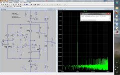
As the doubt about the need of matched transistors appears very often, i post here the same circuit with bc327 for pnp and bc547c for all npn, they are very different and the thd is 0.000008% (7,8ma/100k), its no need for matched transistors. hope this end the subject, and we can move on.
Attachments
How doy you trim away the ofset at the output..??
As i say before (post 108) just increase 6.2ma in the upper current source use a pot in the R3 position, this also serves to trim the output offset. You can add a servo for better offset control .
The increase in 2nd harmonic may be even good sound wise, although distortion of this small magnitude is not likely audible anyway.
")
As far as the balanced output issue, I've never seen a discrete design that gives more CMRR than it adds in 2H and 3H. IC's just completely outperform for balanced to unbalanced conversion, next are transformers, so typically it just doesn't pay to build in a discrete bal-unbal conversion in a DAC analog stage. Probably the smartest is to leave a balanced output to the poweramp where if the output is p-p one can take advantage of having both phases. Or use a good multibit DAC.
That is also my opinion.
I designed a simple MC phono pre-pre with a floating supply based on the principle shown.
I will build it over the weekend.
Keep us informed , hope you like the end result.
The offset current from the DAC-chip makes app 2V offset at the output ..but the circuit does not performance vise seem to run into trouble... In practical terms the offset needs to be addressed...could maybe be done by inserting at counter current at the input, the simple solution would be to use a transformer, but I'd rather not, they cost, and though simple, not very pure.
Problem with a countercurrent at the input is it adds noise to the whole deal (bottleknecks the design), a transformer can really sound great on the output of a DAC stage but this has such good performance I wouldn't want to fog it up with iron. Best bet would probably be a folllowing this I/V with a diamond buffer or other buffer that that can be setup to null the offset with a servo or (preferrably) trimpot. This would allow the use of more/better filtering in between if one prefers.
As the doubt about the need of matched transistors appears very often, i post here the same circuit with bc327 for pnp and bc547c for all npn, they are very different and the thd is 0.000008% (7,8ma/100k), its no need for matched transistors. hope this end the subject, and we can move on.
Sorry about the doubt, soured by years of unimppressive results with open-loop BJT I/V's. It really looks like you have conquered the BJT I/V compromises many of us have been dealing with for years. Thanyou for sharing, please keep us updated as you build it and don't lose patience with our paranoria
. Do you plan on a breadboard first or starting with PCB's ?Hi Zinsula,
i was told that the output impedance of the pcm1794 is 2M with 22pf, try to find in internet for the real value, but no luck
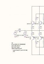
this circuit was design with that in mind, with a source of 1k the distortion is a lot worse (0.008%). but i have made some changes in the input and got 0.000064% thd with 1k input impedance see circuit below
how do you come to 1k
Dug thru my notes and the PCM1794 has an output impedance of 670. which is in line with other high current output S-D DAC's.
The 2M number is way way off any current DAC ever made.
So the best way to spice the PCM1794 would be a current source with app 700 ohm to GND..?? If this is the case, then input impedance really starts to matter.. The voltage source with serial impedance seem just too ideal to match real-world conditions
Textbook current source output impedance is with the output impedance in parallel (to ground on the simulator) but a DAC chip current source doesn't "originate from ground").
Best I've found that models reality is voltage source with series reg. In this case the voltage source would be 3.4pk *780 = 2.625V + 780 series resistance giving a 3.4maPk current sine wave.
Its impossible to model what really comes out of a current output DAC as they aren't square wave but dang close.
So you see that current output DAC chips really aren't current sources unless considered in relation to a opamp I/V' input impedance (virtual ground). Its all relative when defining a current source vs a voltage source, and further shows that modern DAC's are designed specifically for opamp I/V. Most current out DAC's you buy these days are just v-out designs with the internal opamp moved external to allow better specs.
This i/v is special enough that you should consider buying a multibit DAC, at least for comparison.
Last edited:
youre right,designed for opmaps,but few opamps have the high freq response of a discrete stage ,the thing is to remove the resistor between the dac out and input of the opamp
-- so dont listen to that c..p that some LT or Lm opamp is better or more musical,important is the SNR and CMR and of course channell separation,you dont even imagine what opamps you can get for 20 usd,thats 10 high quality dip8
-- so dont listen to that c..p that some LT or Lm opamp is better or more musical,important is the SNR and CMR and of course channell separation,you dont even imagine what opamps you can get for 20 usd,thats 10 high quality dip8
Attachments
Last edited:
Would the offset then be modeled at a separate current source in parallel or simply as a voltage offset on the generator..??
Add a current source to model after the resistor for the offset. Be careful not all DAC's define thier offset the same. Some the offset current is + others - direction, I think the TI's are an oddball, I know the TDA1541 swinggs from 0 to -4mA (-2mA offset) but I think the TI PCM17xx are a positive offset , with S-D dac's it usually works out that they like to see 1/2 their single supply voltage on their output. So a DAC that runs off a +5V rail wants 2.5V DC at the i-out, and a 3.3V rail DAC wants 1.65V. Since PCM17xx run off +5V, you will know you have the right offset current when simulation shows 2.5V at the input to the I/V.
Dug thru my notes and the PCM1794 has an output impedance of 670. which is in line with other high current output S-D DAC's.
The 2M number is way way off any current DAC ever made.
Regal,
What is the source of that 670R figure? I'm not disputing it, it's just that the output impedance of the PCM179X series has been shrouded in mystery because T.I. hasn't seen fit to document it in their datasheets. By the way, the number I've seen reported (unofficially and indirectly) is 100k, supposedly from T.I. engineers in Germany.
Last edited:
here is the circuit with the current mirror, but i don't like it very much.
This circuit gave me an inspiration. Thank you!
I am trying out a "darlington current mirror common base complementary" amplifier... it's has lower THD than my other design, but higher noise. I'm not sure whether or not I'm going to go with it yet.
As the doubt about the need of matched transistors appears very often, i post here the same circuit with bc327 for pnp and bc547c for all npn, they are very different and the thd is 0.000008% (7,8ma/100k), its no need for matched transistors. hope this end the subject, and we can move on.
I tried modeling just the front end (common base portion) of your circuit and I'm getting way too much gain. It's something like 100dB. Of course, I removed the emitter degeneration resistors, and the base stopper resistors as well. Hum ho.
I tried modeling just the front end (common base portion) of your circuit and I'm getting way too much gain. It's something like 100dB. Of course, I removed the emitter degeneration resistors, and the base stopper resistors as well. Hum ho.
Ideally, voltage gain would be much higher, increasing as the virtual ground impedance of the grounded-base stage input is reduced. But what matters here is current flow. The circuit conveys DAC output current to the 400R I/V resistor, while isolating the DAC output from the voltage swing developed across the I/V resistor.
Last edited:
- Status
- This old topic is closed. If you want to reopen this topic, contact a moderator using the "Report Post" button.
- Home
- Source & Line
- Digital Source
- dac I/V convertion with very low distortion