The lme 49811 is class A biased, but only puts out 6mA of current, so, to run the balance of the amp in class A you will need a vbe circuit that will significantly boost the bias current. The 49830 on the other hand makes 50 mA of bias, but the chip itself is biased class a/b, so, it would seem to make much sense to bias what follows the chip in class A.and cannot be achieved by 2 transistors and we just cant restrict to that number though...
rhythmsandy,
Have you looked on this forum and the internet for a proven amp design that my fit your requirements. When or if you make small changes or choose your own design much testing of component compatibility and layout may be required.
The LME chip manufacturer has many useful samples with intensive testing posting on their website which I found quite useful when putting together my small amp with mosfet output devices. I got the frontend boards from a member here who has his own website and much good background information. His name escapes me at the moment. His boards allow for quite a few unique layout configurations so your design will not be a clone.
My LME amp never made it to a chassis or case since I got the tube bug. That was a costly decision. But, are they not all.
Have a nice labor day weekend. Monday off yeah.") Tad
Tad
Have you looked on this forum and the internet for a proven amp design that my fit your requirements. When or if you make small changes or choose your own design much testing of component compatibility and layout may be required.
The LME chip manufacturer has many useful samples with intensive testing posting on their website which I found quite useful when putting together my small amp with mosfet output devices. I got the frontend boards from a member here who has his own website and much good background information. His name escapes me at the moment. His boards allow for quite a few unique layout configurations so your design will not be a clone.
My LME amp never made it to a chassis or case since I got the tube bug. That was a costly decision. But, are they not all.
Have a nice labor day weekend. Monday off yeah.
TadI have OPC's and Panson's versions of the LME498xx chips.
The OPC is currently set for 300mA of output bias on a 0.6C/W sink with +-45Vdc at the PCB.
I tried last night using a higher bias of 450mA to see how hot it got. I was not happy, I could not hold my fingers on the ends of the sinks, never mind the centre where the devices are located.
I could try taking out the 30+30Vac transformer and replacing it with 25+25Vac, or 16+16Vac and biasing higher, for similar heatsink temperatures. I don't have any around the 20+20Vac level.
At present the 300mA gives ~ 1.4W of ClassA in a 70W ClassAB amp assembly.
450mA would give ~ 3.2W of ClassA in a 40W ClassAB assembly, if I use the 25Vac transformer.
The 16+16Vac would probably result in about 9W of ClassA in a 25W ClassAB.
If I doubled the heatsink to 0.3C/W I might just about get 15W to 20W of ClassA from the single pair of 250W devices.
Last edited:
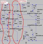
I modified the output power board to accommodate a CFP output stage. It consists on MJE15034/35 and MJL21194/93. The driver collector resistor is initially 120 R. Re is 0.22 R. Base stopper for driver is 100 R. The stopper very important here to avoid oscillation. The comp cap is 32 pF. Bias is simply generated by two diode and a trim pot. Each diode is attached to the driver heatsink as shown in the picture. Output coil and damping is employed.
Compared to emitter follower output stage, CFP is relatively less friendly. This is my impression at the moment.
THD+N vs freq (BW=80k) for 18W/8R and 36W/4R is shown in the picture.
.
Hello Panson ,
CFP performs always better in thd terms also at high freq when they are biased correctly .Also they need less bias current for same thd compaired with emitter follower .
For a proper biased cfp ,the output stage needs 10-12mA and the drivers 10-20mA .Then is important to not have any stray inductance in the cfp circuit ( local negative feedback ).
Also the driver needs to have a lower load ,maximum 56 ohms for low thd .22ohms will decrease the thd by a half than 56ohms .120 ohms is very high .
Last edited:
Also I forgot to tell that in cfp/sziklai configurations it is also important to have low capacitance between collector and base at least for the drivers,the Cob parameter .2sc5171,2sa1930 are low cob and great for sziklai configs .
The lowest thd I obtained with 22 ohms load for driver collector ,12 mA in the power transistors.The cfp had drivers 2sc5171 and power bjt 2sc5200 which has also lower cob compaired to all others .In this configuration the thd at 20khz is the smallest possible < 0.000 %.
The otput stage is present here : http://www.diyaudio.com/forums/solid-state/135122-wonderfull-sziklai-26.html#post3258858
The power resistors 0.22 ohms should be non-inductive .
This can be done with Lme49810 because the chip has pre-drivers already .
This kind of project will be my next ,Lme49810 + cfp output with 2sc5171/1930 and 2sc5200/1943 .If you have some small Cob drivers I am very interested to see the results .
I am extremely curious how is the pattern of the thd with these devices .
Also I saw that you have obtained higher thd with a Lme supply non regulated (10ohms+cap) .From what I guess the chip has low psrr on the negative rail .It would be great if you can run the same test but with the filter inserted only for the negative rail .
Last edited:
can LME49810 be used for class A? as the previous posts say that LME49830 itself is biased in A/B. I agree 811 works in class A but how about 810?
Both chips has the vas biased in class A .811 has the output direct from the vas stage.The 49810 added an emitter follower to provide a higher current at the output .So the 810 has the vas in class A like 811 but also an simple class A/B emitter follower stage .
Both chips has the vas biased in class A .811 has the output direct from the vas stage.The 49810 added an emitter follower to provide a higher current at the output .So the 810 has the vas in class A like 811 but also an simple class A/B emitter follower stage .
so the 810 vas might be in class A but the emitter follower at its output would not run in class A if biased at the output stage isnt it?
Here is a similar example,hope that it helps ,To have triple output stage at 811 you must add 6 transistors .To have triple on 810 you must add only 4 transistors because 2 are already in it .
can you attach the spice file i would like to simulate few things..
Hi everyone at DIY,
Sorry I have not posted for quite some time but I just got a notice in my email about a comment on this thread and thought I could shed a little light on the questions posted here...
The LME49810 was designed for high power amplifiers for the music industry and a class AB stage was added to its output stage to bring the output current up to 50ma (60max on data sheet) to be able to achieve 2KW with a single Darlington output stage. It also has a pure Baker Clamp which is only slightly different than a similar circuit implemented in the LME49811 and LM4702.
The LME49811 is a class A internal implementation but it only has 7ma of output current. It also has a "Bob Pease" improvement to the layout of its input stage to improve low level thermal performance. We did this when we split the stereo LM4702 in half to create the LME49811, that I specified.
I have been listening to the LME49811's used in a mono block amplifier design, very similar to the circuit in app note AN-1490 for the stereo LM4702, at home and here in our sound room at TI Santa Clara for over 5 years now. With 50VDC rails that amplifier has no trouble driving our Wilson Watt Puppy model 7's at work. You can see from the graph in AN-1490 (for the very similar stereo LM4702) that this amplifier design achieves 0.0005% THD+N. Actually my LME49811 amplifier measures even better than that.
Best TI Audio Regards,
Mark Audioman54
Best TI Audio Regards,
Ya did that "reverse Joad family commute" in which so many Californians now find themselves. Welcome back!
An externally hosted image should be here but it was not working when we last tested it.
Hi everyone at DIY,
Sorry I have not posted for quite some time but I just got a notice in my email about a comment on this thread and thought I could shed a little light on the questions posted here...
The LME49810 was designed for high power amplifiers for the music industry and a class AB stage was added to its output stage to bring the output current up to 50ma (60max on data sheet) to be able to achieve 2KW with a single Darlington output stage. It also has a pure Baker Clamp which is only slightly different than a similar circuit implemented in the LME49811 and LM4702.
The LME49811 is a class A internal implementation but it only has 7ma of output current. It also has a "Bob Pease" improvement to the layout of its input stage to improve low level thermal performance. We did this when we split the stereo LM4702 in half to create the LME49811, that I specified.
I have been listening to the LME49811's used in a mono block amplifier design, very similar to the circuit in app note AN-1490 for the stereo LM4702, at home and here in our sound room at TI Santa Clara for over 5 years now. With 50VDC rails that amplifier has no trouble driving our Wilson Watt Puppy model 7's at work. You can see from the graph in AN-1490 (for the very similar stereo LM4702) that this amplifier design achieves 0.0005% THD+N. Actually my LME49811 amplifier measures even better than that.
Best TI Audio Regards,
Mark Audioman54
The only problem I see is the slew which is 15v/us and that is relatively low when compared with 810. Is it possible to get more slew out of 811? like 50v/us.
I am fixing with 811 as its more pure. Like I said If its possible to get more slew then its fine is that internally fixed?
I do agree that we dont require more slew in general but on selling front it makes big different.. and to be precise the slam will be great...
- Status
- This old topic is closed. If you want to reopen this topic, contact a moderator using the "Report Post" button.
- Home
- Amplifiers
- Chip Amps
- Comparing LME49810, 49830 and 49811