I made some changes to the schematic.
I lowered the VAS quiescent current to 8.8 mA due to nasty current spikes on the bases of Q18/Q19.
I removed the two schematics in the top of the thread because they aren't needed anymore (and I'm running low on space).
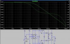
Here are some simulations:
Closed loop gain

Open loop gain

I lowered the VAS quiescent current to 8.8 mA due to nasty current spikes on the bases of Q18/Q19.
I removed the two schematics in the top of the thread because they aren't needed anymore (and I'm running low on space).
Here are some simulations:
Closed loop gain
Open loop gain
I think the open loop gain is telling you that the amp is unstable.
The slope of the HF response increases just before the gain drops to 0dB. and there the phase is greater than 180degrees. I think that means you have simulated an oscillator.
How did you get open loop gain flat from 1Hz to 2.5kHz?
The slope of the HF response increases just before the gain drops to 0dB. and there the phase is greater than 180degrees. I think that means you have simulated an oscillator.
How did you get open loop gain flat from 1Hz to 2.5kHz?
The point where the two gain curves first intersect is ~1.6 MHz. Isn't that the point you should look at for phase margin or have I misunderstood?
I simulated the open loop gain with R1 and C1 removed.
C2 and C8 set to 1000000uF and R15 set to 0.001R.
R36=20R, other than that the simulation is done with the circuit in the schematic above.
The closed loop simulation is done with R1 and C1 removed and R36=20R.
Don't know why it's flat from 1 Hz to 2.5 kHz.
I presume lower roll-off @ 1Hz is because of some low pass filter and upper roll-off @ 2.5kHz is the first pole set by Miller compensation. By looking at the pictures the amp seems to be unstable. The easiest way to make it stable again is to increase the Miller capacitor.
Lets call the above open/closed loop plots for:
Open loop: AOL
Closed loop: AFB
I exported them from LT Spice into MATLAB and did the following:
BetaAOL = (AOL - AFB) / AFB
I then plotted the magnitude and phase for BetaAOL.
The result:

I like the results except for the "hump".
I then tried increasing the miller caps to 100pF. No "hump" suppression there. So I tried increasing the 68R degen resistors in the diff pairs to 100R. This helped a bit.
The result:

The last plot is telling me that the amp is quite stable. However I'm a bit concerned about the "hump" it's still pretty close to unity gain.
Or could it be that I have misunderstood something critical and my phase and gain margin calculations are wrong?
Open loop: AOL
Closed loop: AFB
I exported them from LT Spice into MATLAB and did the following:
BetaAOL = (AOL - AFB) / AFB
I then plotted the magnitude and phase for BetaAOL.
The result:
I like the results except for the "hump".
I then tried increasing the miller caps to 100pF. No "hump" suppression there. So I tried increasing the 68R degen resistors in the diff pairs to 100R. This helped a bit.
The result:
The last plot is telling me that the amp is quite stable. However I'm a bit concerned about the "hump" it's still pretty close to unity gain.
Or could it be that I have misunderstood something critical and my phase and gain margin calculations are wrong?
AndrewT said:I don't think the current mirror on the LTP collectors will be effective with the parallel 680r load.
Without the 680r the circuit does not work.
Without the current mirror the circuit does work, but badly.
Well done right it actually performs significantly better than a standard complementary input stage.
I explained why (with actual technical reasons) here:
http://users.picknowl.com.au/~glenk/K12A.HTM
danfo098 said:Lets call the above open/closed loop plots for:
Open loop: AOL
Closed loop: AFB
I exported them from LT Spice into MATLAB and did the following:
BetaAOL = (AOL - AFB) / AFB
I then plotted the magnitude and phase for BetaAOL.
I like the results except for the "hump".
I then tried increasing the miller caps to 100pF. No "hump" suppression there. So I tried increasing the 68R degen resistors in the diff pairs to 100R. This helped a bit.
The last plot is telling me that the amp is quite stable. However I'm a bit concerned about the "hump" it's still pretty close to unity gain.
Or could it be that I have misunderstood something critical and my phase and gain margin calculations are wrong?
Hi
I'm not immediately sure what is happning in your sim to cause that hump, but I just ran a simplified sim of your amp to check the compensation. This is very similar to an amp I already have in my LTspice file, so all I had to do was change a few component values. I did, though, make some minor changes which I think are necessary.
In order to minimise LTP imbalance due to Vbe differences between the PNP and NPN VAS transistors you really need to swamp these out by having at least a volt of emitter degeneration.
This means, for a VAS standing current of 10mA, a total of 100 ohms emitter degeneration is required for each VAS transistor.
Attached below is a loop gain / phase plot for your amp. All the values are the same....
3mA LTP tail current
68R LTP emitter degeneration
680R LTP load resistors
56pF Cdom's
....except I have increased the VAS emitter degeneration to 100 ohms and increased the VAS biasing current source to 3.4mA to give a VAS standing current to 10mA.
The plots look fine (no hump) and the unity loop gain frequency matches your sims, at approximately 1.2MHz.
Note though, that 1.2MHz is pushing it a bit for a real amp, unless the layout is very good. You will definately need an output inductor to isolate any capacitive load.
82pF would probably be safer for Cdom, returning a unity loop gain frequency of around 800kHz.
I would also recommend that you introduce R-C filtering on each supply rail to filter / isolate the ripple induced on the supply rails by the output stage from the VAS and LTP.
Cheers,
Glen
Attachments
re. latest version shown in post21.
I like the way you show all the data for the set up in addition to the schematic.
How does one decide what CCS current to set to ensure the correct voltage drop across the 680r.
Glen,
thanks for that link explaining 680r & CM for the LTP.
I like the way you show all the data for the set up in addition to the schematic.
How does one decide what CCS current to set to ensure the correct voltage drop across the 680r.
Glen,
thanks for that link explaining 680r & CM for the LTP.
AndrewT said:How does one decide what CCS current to set to ensure the correct voltage drop across the 680r.
It's just the voltage you want / 680R.
AndrewT said:Hi,
is that the same as saying use the CCS current across the 680r to set the VAS quiescent current?
Sounds too easy!
picknowl is bookmarked.
Yes. The LTP current is actually irrelevant.
Back home again.
Here is the latest schematic.
Removed the collector resistors for Q19/Q20.
Added 2 pole compensation.
Added cascodes in the VAS.
Changed VAS emitter degeneration to 100R.
Changed diff-stage emitter degeneration to 100R.
Added RC filtering for diff/VAS supply.
Lowered supply filtering capacitance to 470uF due to size constraints.
Added two Leds.
The "hump" however remains but I'm not going to spend more time on it for now (maybe it's because of the on-semi transistor models?).
LT Spice loop gain simulation.
The PCB size is 120x70mm (~4.72"x~2.76").
Preliminary PCB component layout.
And finally the BOM.
I finished the PCB.
Schematic and PCB.
PCB Specs:
120x70x1.6mm
6 layers
70um copper on all layers
ENIG plating
$40.8 US / card (10 card order)
The PCB:


Schematic and PCB.
PCB Specs:
120x70x1.6mm
6 layers
70um copper on all layers
ENIG plating
$40.8 US / card (10 card order)
The PCB:
For that kind of symmetrical LTP with two current mirrors I did some experimentation a few years ago with an optocoupler for VAS bias regulation. One of the problems that I had was that 4N25 was very slow, I didn't know about 6N135, 6N136 and HCPL4502 back then 
The photodiode was in series with the collector of the Vbe multiplier and with a resistor in parallel.
The photodiode was in series with the collector of the Vbe multiplier and with a resistor in parallel.
So I could remove R22/R23 and their respective CCS:es and use a optocoupler instead somehow and get better performance?
I'm not sure how I should connect the feedback from the optocoupler so feel free to give more information, but if the performance enhancement isn't really great I think I'll stick to the current design.
Also I found a mistake in the pcb above (the E and B in the MJE340/50 footprint was inversed) but it's fixed now. I also removed one via, so now there is a total of zero vias.
I'm not sure how I should connect the feedback from the optocoupler so feel free to give more information, but if the performance enhancement isn't really great I think I'll stick to the current design.
Also I found a mistake in the pcb above (the E and B in the MJE340/50 footprint was inversed) but it's fixed now. I also removed one via, so now there is a total of zero vias
.Yes, I was talking about bias control in symmetrical VAS with two current mirrors.
The trick would be to make a circuit that always tends to bias runaway and then use one or two matched optos to reduce bias to the desired level.
For example, adding B-E resistors (or current soruces) to the VAS transistors to drain any minimum error current from the mirrors and then a current source between the bases which should be progressively turned off as the opto turns on.
It involves some complexity, but it kills the symmetrical-VAS-with-two-mirrors myth (In fact, I wouldn't do it for any other reason, as I would prefer to do a class D amplifier to start with).
The trick would be to make a circuit that always tends to bias runaway and then use one or two matched optos to reduce bias to the desired level.
For example, adding B-E resistors (or current soruces) to the VAS transistors to drain any minimum error current from the mirrors and then a current source between the bases which should be progressively turned off as the opto turns on.
It involves some complexity, but it kills the symmetrical-VAS-with-two-mirrors myth
(In fact, I wouldn't do it for any other reason, as I would prefer to do a class D amplifier to start with).- Status
- This old topic is closed. If you want to reopen this topic, contact a moderator using the "Report Post" button.
- Home
- Amplifiers
- Solid State
- Comments on this symmetric design