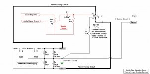
.
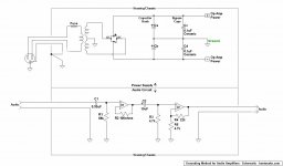
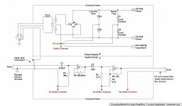
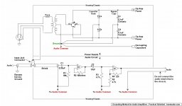
Would anybody like to comment on the grounding scheme posted below?
The principle here is to minimizer audio distortion by keeping the audio signal away from power supply voltages and currents. But at the same time the entire cicuit must be grounded with a "safety ground" which does connect audio to power, creating a contradictory situation.
This contradiction is dealt with in various ways by various gurus. The goal in the circuits posted below is to comply with every mandate laid down by every guru there is, individual or corporate. The circuits are intended to be not schematic, but practical, showing real-world wiring and connections.
All three circuits are electrically the same. The first is for reference, drawn using the customary schematic symbols. The following two circuits are practical, the difference between them is whether a shielded input conductor is used.
If I've made mistakes, or have misunderstandings, I'd be very glad to hear about them. Looking forward to hearing about what I've missed, misinterpreted, or just plain not caught onto.
.
Attachments
Fourth option. This is a more audio friendly layout.
Smaller audio loops. Smaller power loops. Moved PSU GND. Removed input ground loop. Removed high inductance (one for all channels) decoupling GND. Added GND loop breaker. Moved mains earth chassis connection.
Smaller audio loops. Smaller power loops. Moved PSU GND. Removed input ground loop. Removed high inductance (one for all channels) decoupling GND. Added GND loop breaker. Moved mains earth chassis connection.
Attachments
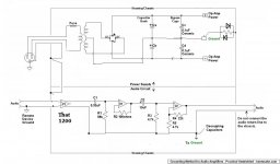
Fourth option. This is a more audio friendly layout.
Smaller audio loops. Smaller power loops. Moved PSU GND. Removed input ground loop. Removed high inductance (one for all channels) decoupling GND. Added GND loop breaker. Moved mains earth chassis connection.
I've used this scheme in commercial units. The chassis is 'loosely' connected to signal ground using small value (<10 Ohms) resistors and having the power company ground hard tied to the chassis as required by code. No problems at all. Best rule is never use the chassis as a conductor, only as a shield.
G²
.
I'd hoped for either validation or--much better--reasoned dissent. Both lacking, I abandon this thread.
However, Google never forgets. So for the benefit of shadetree techs yet unborn I feel duty bound to give at least some some explanation of the reasoning and purpose behind the grounding scheme(s) I posted. Hence the following references:
This Texas Instruments article seems to have at least some acceptance in this forum. Google for, "Grounding Principles, Bruce Trump, May 21 2013" including quotes, or here's the link: Grounding Principles - The Signal - Archives - TI E2E Community
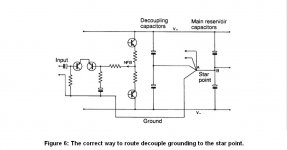
The first illustration below is from Douglas Self's, "Self on Audio." This is figure 6 in Chapter 21, section titled, "Distortion 5: supply ground loops," page 272. Note the separation of the capacitor bank return from the decoupling cap return, and the provision for additional returns to what Mr. Self calls the star point. Do not fail to study Mr. Self's explanatory text notes.
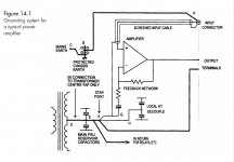
The second illustration is from the same Mr. Self's, "Audio Power Amplifier Design Handbook," Chapter 14 titled, "Grounding and practical matters," section titled, "Power amplifier PCB layout details," page 402. This illustration gives perhaps the best overall view of the concepts involved.
Especially important here are Mr. Self's text notes throughout the chapter, in which he explains, among other things, why the audio-to-chassis ground connection should be made at the input connector.
I hope these might be of some interest.
I CLAIM FAIR USAGE of the quoted materials on grounds of: 1. Their usage is for educational purposes, and: 2. No profit accrues to me.
.
I'd hoped for either validation or--much better--reasoned dissent. Both lacking, I abandon this thread.
However, Google never forgets. So for the benefit of shadetree techs yet unborn I feel duty bound to give at least some some explanation of the reasoning and purpose behind the grounding scheme(s) I posted. Hence the following references:
This Texas Instruments article seems to have at least some acceptance in this forum. Google for, "Grounding Principles, Bruce Trump, May 21 2013" including quotes, or here's the link: Grounding Principles - The Signal - Archives - TI E2E Community
The first illustration below is from Douglas Self's, "Self on Audio." This is figure 6 in Chapter 21, section titled, "Distortion 5: supply ground loops," page 272. Note the separation of the capacitor bank return from the decoupling cap return, and the provision for additional returns to what Mr. Self calls the star point. Do not fail to study Mr. Self's explanatory text notes.
The second illustration is from the same Mr. Self's, "Audio Power Amplifier Design Handbook," Chapter 14 titled, "Grounding and practical matters," section titled, "Power amplifier PCB layout details," page 402. This illustration gives perhaps the best overall view of the concepts involved.
Especially important here are Mr. Self's text notes throughout the chapter, in which he explains, among other things, why the audio-to-chassis ground connection should be made at the input connector.
I hope these might be of some interest.
I CLAIM FAIR USAGE of the quoted materials on grounds of: 1. Their usage is for educational purposes, and: 2. No profit accrues to me.
.
Attachments
Last edited:
Dear Bentsnake,
Now that you have named your sources it will be easer to explain why the differences in layout. The TI layout (figure 2 of TI link) doesn't take the inductance of the ground trace/wire into consideration. The decoupling capacitors plus the inductance of the ground connections form a Low-pass filter (CL). The ability of the capacitors to supply current to the opamps and receive current from the PSU is severely reduced. There will probably be oscillations caused by the higher inductance but this will also depend on the components used. Please do the simulations. I also cant see how to design this without creating larger loops.
Perhaps you could post some links of PCB designs or amp designs that use multiple connections between the PSU GND and the AMP GND.
In the past I have looked at the PCB layouts of the D. Self power amps and he uses a completely different layout. He likes to have large +Power/-Power/GND loops, placing the positive and negative decoupling (and the power rails) as far apart as possible with each decoupling capacitor having its own trace to PGND. On at least some of his designs he has the output return very close to where the PGND enters the PCB and places the input GND as separate as possible.
Last edited:
Several of us have pointed out weaknesses in your proposals and suggested an alternative. For example:bentsnake said:I'd hoped for either validation or--much better--reasoned dissent. Both lacking, I abandon this thread.
In what way does this fail to be "reasoned dissent"?DF96 said:Yes, all the circuits in post 1 inject PSU charging pulses into the audio ground. Post 2 is the way to go.
.
I'd hoped for either validation or--much better--reasoned dissent. Both lacking, I abandon this thread.
However, Google never forgets. So for the benefit of shadetree techs yet unborn I feel duty bound to give at least some some explanation of the reasoning and purpose behind the grounding scheme(s) I posted.
Wow, what a sack-bag.

No ground loop breaker?
Can the ground loop breaker and THAT1200 be omitted and use a Star Ground (near the PSU output) with wire running from the Earth and Audio Gnd?
I am not sure what the THAT1200, quick search shows it's a balanced line receiver? Looks like it isolates the input/remote audio device ground from our circuit. Can I do without it?
Attachments
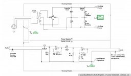
This was just an example of a grounding layout. As a design/layout it is incomplete.
What do you want to build?
Mark,
I have two project in mind.
Amplifier with 3 separate components/pcbs:
- Transformer
- Linear PSU
- Single Amp Board
DAC unit with 6 separate components/pcbs
- Transformer
- Linear PSU
- Regulator PSU
- USB reciver Module
- DAC module
- I/V Stage Module
I have looked inside my high end CD players quite a bit and it looks like the standoff are grounded to the whole chassis, and there are grounds running from board to board and everything is interconnected, and it looks like there are a ton of ground loops but Star Ground looks like the only logical choise in these forums. Also I've seen those ground loop breaker circuits being used quite a bit (including myself in one application)
First design a good audio layout. The audio signal and its return. Include the feedback loops. If you have more than one channel then draw at least two of them. What is the best ground/return layout to achieve good audio? Locate the current loops in the schematic and keep them small on the PCB.
Then design the voltage supplies and return, the decoupling capacitors and power connections. Do you need multiple voltage supplies and how should they be connected to the devices and ground? LTSPICE is a good tool to see how the different PSU components interact.
Trace the current flow in the schematic and/or PCB design. Start from the (voltage supply) decoupling caps, to the devices, to the load, to the decoupling caps return, don't forget the feedback loops. The goal is to keep the loop area small. Which means short and thin.
Most of the design information can be found in the device datasheets. There is nearly always a schematic, PCB and description to help you with your layout.
Add the mains EARTH/GND to chassis and chassis to amp GND connections. Reduce the current flow between the chassis and the amp ground. A ground loop breaker does this.
A system schematic with the ground connections will help in tracking down potential problems. Look at the way Bentsnake has connected the mains earth to the input ground. As a single channel it may look OK. When you add a second channel, two additional ground loops are created, one with the upstream equipment and one through each of the connections to audio common. It is both of these ground loops that cause hum and other problems. If you can trace a parallel route for the signal grounds or supply grounds you have designed a ground loop.
Last edited:
Since you (bentsnake) said you were looking for answers...
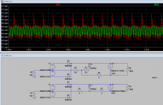
Consider the pic attached. It's a simplified power supply but it will establish the principles. The 1R and 0.5R resistors simulates the wires' resistance. Ignore R6-R7, they only establish a reference for the simulator. The currents through R8-R9 show what happens accross the audio loads (I1-I2)
The top setup is what you are proposing. See how we have 100hz spikes ?
The bottom setup is what has been suggested in post 2. See how those spikes disappear ?
Attachments
<< The top setup is what you are proposing. >>
No, it's not, it's something entirely different.
.
It's functionally identical to a single rail version of your scheme. Explain why it would be "entirely different" ?
To say it otherwise. Look at the first post, third pictures. The "common" ground is halfway on the wire going from the CT to the reservoir caps. This is what is illustrated as wrong in my sim and what post 2 corrects.
Last edited:
.
<< It's functionally identical to a single rail version of your scheme. >>
So it turns out that a half-wave, single-rail circuit is functionally identical to a full-wave, dual-rail circuit? Forgive me if I think not.
Which at once tells us that further discussion would become an argument over the meaning of "function." Absolutely no point in going there.
<< Explain why it would be "entirely different" ? >>
That's not how it works. You make a claim, it's up to you to back it up.
Or not, of course, as you choose.
I vote not. For the following reason.
<< [In the posted circuit the] "common" ground is halfway on the wire going from the CT to the reservoir caps. This is what is illustrated as wrong in my sim and what post 2 corrects. >>
In the circuit I posted there's nothing identified as "'common' ground," also no reservoir caps, so I can only guess at your meaning.
Even so I think I've got this figured out. Simple confusion arising from the fact that my schematic is not to scale. Ummm...what schematic ever is, was, or will be to scale?
Please consider that the point identified as "Ground" is as close as possible to the transformer.
.
the sim IS a full wave, think again and come back... The problem shown here will also show in a dual rail sim. Why don't you try for yourself ?.
<< It's functionally identical to a single rail version of your scheme. >>
So it turns out that a half-wave, single-rail circuit is functionally identical to a full-wave, dual-rail circuit? Forgive me if I think not.
ANY power supply has reservoir caps. Otherwise you would have pulsed DC and not DC. Read Self again and come back. Audio common, common gnd, same, same. Don't turn all semantics.In the circuit I posted there's nothing identified as "'common' ground," also no reservoir caps, so I can only guess at your meaning.
Which is the worse place ever to put it. It's not a matter of scale anyway and your schematic is supposed to be a wiring guide, remember ? If you want to put "gnd" close to the transformer, you didn't figure anything yet.Even so I think I've got this figured out. Simple confusion arising from the fact that my schematic is not to scale. Ummm...what schematic ever is, was, or will be to scale?
Please consider that the point identified as "Ground" is as close as possible to the transformer. .
A simple exercise for you: draw the current loop for an audio signal and for the loop charging the capacitor on your schematic. I'm afraid you don't realize the audio loop doesn't pass through the center tap of the transformer.
Fourth option. This is a more audio friendly layout.
Smaller audio loops. Smaller power loops. Moved PSU GND. Removed input ground loop. Removed high inductance (one for all channels) decoupling GND. Added GND loop breaker. Moved mains earth chassis connection.
This is a dangerous proposal (and technical it makes no sense too - go to a Class-2 design if you want the ground float)!
Read the relevant legal restraints before using a ground breaker.
Think of what happens if the transformer has a fault and 230 V appear at the output?
Can you be sure that the circuit breaker will not be blown before a 35 A fuse?
At least use small fuses on your power inlet and a Class-2 transformator.
And be prepared to justify your abondon of "the state of the art" at court if something terrible happens...
Thx, Udo
- Status
- Not open for further replies.
- Home
- Source & Line
- Analog Line Level
- Comment on Grounding Scheme?