@Eva:
@ Topic
I have to apologize, we lost you again.
OOps, sorry I didn't meant.

May she just don't like there are some people still use classAB, or even old classA pentodes. That she thinks they are doing wrong way. Also their reasons just old.

Just like SS vs Tubes debate, They always says that there is something from tube amp that they think not present at any solidstate, did you know it is distortions.
But it's a nice face *alwaysproudonmyown*
That's all you need.Ontoaba,
I talk like a hypochodric nerd again, don't I?
.... Dunno may be yes or not, just don't disturb your neighbor, if you want peace coming at your heart.
I hope you're all digital people are just fine right there.
Markus
See below.
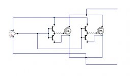
It is the source inductance IN THE GATE DRIVE LOOP that really matters because it provides necessary feedback during current slope. Keep source power path and gate drive path separate. SHould do.
Better to use separate buffer EF drivers for each mosfet with kelvin source contacts and the gate driver return must be routed to common route access to all source terminals such as -Ve rail or switching node while keeping the source traces symmetric and get rid of unwanted voltage drops due to parasitic inductance. This scheme works well for me.
Attachments
Last edited:
Hi Kanvar,
your arrangement is making sense to me and your comment of keeping the source traces symmetric is exactly the point I was waiting for, when asking for a specific layout.
But I do not think that you generally get rid of parasitic inductive voltage drops.
Your arrangement is forming a well defined di/dt limiter.
di/dt is defined by the geometry of your symmetric source traces, lead inductance of the MosFet package (again source), treshold voltage and Rds vs Ugs charakteristic of the MosFet and the driver supply voltage.
But I do not think that you generally get rid of parasitic inductive voltage drops.
Hi Choco,
Voltage drops are always there due to unavoidable parasitics but one can balance out the effect if the traces are similar enough to minimize the imbalance in voltage drops. The unwanted imbalance in voltage drop leads to drastic change in conduction of current between paralleled devices.
but one can balance out the effect if the traces are similar enough to minimize the imbalance in voltage drops.
...fully agree. The remaining downside in paralleling like proposed by darkfenritz or like you , is that there is one parameter more to be handled when doing the layout, but of course possible.
My personal taste is to stay without paralleling as long as I get a strong enough device in the TO220 package.
TO247 is much less convenient for fast switching and for snubbering (played around with IRFP4668). Consequently paralleling devices appears attractive to me in designs where a single TO220 will not be sufficient anymore.
Ontoaba,
You are getting old ?
No, just almost between young and old.
dark using interleaved, not paralleling. Inductor is giving drop voltage at charging and extra voltage on discharge. I prefer shortest sources connections if using balanced traces. Like in 2in1 RF power fets.
- Status
- This old topic is closed. If you want to reopen this topic, contact a moderator using the "Report Post" button.
- Home
- Amplifiers
- Class D
- class D vs class AB current capability.