wow, what a circuit ")
One thing I found interesting:
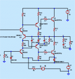
During the negative swing the diode "D" is sinking all the current driven through the load, thus droping some 0.7V or so, thus turning off T7, thus the only thing that keeps the negative swing going is the 250µ bootstrap cap.
Really a tempting design.
One thing I found interesting:
During the negative swing the diode "D" is sinking all the current driven through the load, thus droping some 0.7V or so, thus turning off T7, thus the only thing that keeps the negative swing going is the 250µ bootstrap cap.
Really a tempting design.
Yes this is the purpose of the bootstrap cap. I think another feature that is significant for sound quality is that the large currents flow outside of the PCB as the 2N3055 are wired on the heatsink and the diode D sits also on the heatsink. It could be the crossover distortion that appear at power >30 watts are due to a a loss of capactity and deterioration of the bootstrap cap. I wonder how this circuit performs with power BJTs featuring a much higher fT than the 2N3055.
I'm a little swamped at the moment, but I am definitely planning to do some simulating research on this circuit to find out its potential.
On the bootstrap cap:
I guess it would be no problem to simply increase its value if it is really running out of charge at high power and maybe low frequency.
On the bootstrap cap:
I guess it would be no problem to simply increase its value if it is really running out of charge at high power and maybe low frequency.
I found in sims that the size of the bootstrap cap is important to distortion; 22uF I found to be optimal when using a Baxandall diode between output and emitter of pnp driver.
Lowest THD is part of the story, I think you are absolutely right about profile of the harmonics. Using good quality sims with good models, I suspect monotonic decreasing, H2>H3> H4 etc is the best profile.
Significantly, this is essentially a quasi-comp output stage, driven from a Rush Cascode, with its phase reversed outputs. But there is still a fair range of current through the RC; with +20dBU output, I saw a range from 0.68mA to 1.05mA, which impacts on Vbe for the RC be junctions. If this range could be greatly reduced, then distortion overall would be lower.
Cheers,
Hugh
Hum...it is becoming a bit intransparent...could you provide the sims schematic?
I think in terms of the original schematic , a fully complimentary design would not provide advantages. It is a long time ago when I was involved in theory of semiconductors but the fundamentals haven't changed devices being complimentary in every respect are impossible due to the different modes of conduction the electron hole stuff and the different carrier mobilities.
I think in terms of the original schematic , a fully complimentary design would not provide advantages. It is a long time ago when I was involved in theory of semiconductors but the fundamentals haven't changed devices being complimentary in every respect are impossible due to the different modes of conduction the electron hole stuff and the different carrier mobilities.
No problem, attached.

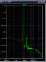
Total Harmonic Distortion: 0.004540% at +20dBU (14.5Vp) into 8R, a respectable figure.
R1, R2 and R3 are all critical; current through the RC is very touchy. The circuit has considerable OLG at the RC outputs; oscillation is a very real issue yet compensation is not used.
I also found, unsurprisingly, that reducing the bootstrap seriously increased distortion at 20Hz. A compromise at around 100uF seems best, but empirical adjustment would be needed as there will be subjective effects on the bass due to the distortion (up around 0.12% with 22uF).
A fully complementary output stage is certainly possible and it would reduce thd considerably, but at the cost of even order distortion, which is musical if not in large quantities. I'd be surprised if it sounded as good.
Cheers,
Hugh
Last edited:
Thanks.
Why is there no Baxandall clamp at the emitter of Q4? Does it make any sense
to have about 100 Ohms resistor between v out rail and the junction of the base of Q2 and C2?
About oscillation...could it be that the rather slow 2N3055 in the original design prevents oscillation ( I think just the opposite but my amp shows no oscillation under various loads ).
Anyway the THD is impressive that points to absence of switching distortions.
If it were not for possible oscillations this amp promises to be one of the most easy to built... however if it oscillates it will cost a bunch of power BJTs.
Why is there no Baxandall clamp at the emitter of Q4?
While both upper and lower device pairs are complementary feedback pairs (Sziklais), the output from the top is taken from the emitter of slave, whilst at the lower pair it's taken from the collector of the slave.
These circuit conditions are very different, with the upper pair used as a phase inverted, and the bottom with no phase change. The upper output device is used in emitter follower and the bottom in common emitter, so there is a requirement in the bottom pair to compensate the absence of a hefty BE junction between driver and output device, hence the Baxandall diode on one side but not the other.
Does it make any sense to have about 100 Ohms resistor between v out rail and the junction of the base of Q2 and C2??
If you mean a base stopper, maybe.....
Hugh
Whats up, guys ??
This is the first even remotely interesting circuit that I have seen at DIYA in a long time.
Attached below is the .ASC (self contained models - ready to run). also , I really would like to make this fully complimentary and able to run with 75v rails (next generation simulation). As it is , it works ... does not switch (see below). I had to offset the AC source 1.25v and added 2 -.1R emitter resistors to see whether it switched , but I seem to have gotten the same results ... no switching and .004-.006% thd. FFT is strange, too...
A VERY different circuit in every way !!!
OS
Attachments
Last edited:
many Tx for your contributions.
Frankly when I built this I had some inclination to maths but I had no idea what I was doing
yet the amp worked from the first moment on...this is a VERY STRONG argument for this design.
Now why is oscillation an issue? It could be if one of the power BJTs turns off but apparently it doesn't. Given the hfe/ic characteristic of a LAPT power BJT (hfe being complex) I think it is a matter of proper choice of the BJTs.
The schemo contains at least 2 errors: emitter of CCS shorted on emitter of output transistor, and 250uF Miller compensation cap instead of 250 pF one.
That capacitor is a bootstrap, not a Miller compensation.
Hi
Piercarlo
Ah yes indeed that explains how no crossover distortion appears even with class B setting of the power BJTs. It appears the same design idea is realized in the old QUAD 303? But why the bootstrap? And indeed the emitter of the current source is forced to -34.4 volts same as the base. If I hadn't built in 1976 I were sure it cannot work but since I have I see it works...
Say "no crossover appear even... " etc. require a bit of explanation because iinstead crossover distortion exist but it's heavily counteracted by strong local NFB factor applied on both halves of output stage. At low frequencies the circuit should work fine, but at higher frequencies, where on.off speed limit of output devices are involved, im not sure if it work very well same as it work at lower frequencies.
Hi
Piercarlo
Peter,
I think it switches all right...... maybe a false dawn, BUT, the transfer kink at crossover is extremely well handled, as good as anything in AB I have ever seen.
Hugh
No, not a false dawn. Just a different form of a concept yet largely applied: use of big NFB factor in order to clean away the most of crossover distortion - and not a really "non-switching" circuit as claimed by its title. The real interesting thing is not the undue "no-switching" attribute but the way of applying to a quasi complementary outtput stage the strategy usually applied in complementary triplet stage (or Sziklay output boosted stage as i prefer call it), where the output stage beneficiate of a dedicated, local NFB loop for linearizing it and its crossover distortion.
Hi
Piercarlo
Hum...if no triplet is ever turned off it doesn't switch. Or better shouldn't.Peter,
I think it switches all right...... maybe a false dawn, BUT, the transfer kink at crossover is extremely well handled, as good as anything in AB I have ever seen.
Hugh
That is the circuit idea. Hence the NFB factor remains constant around signal zero crossing. At least as far as I understand the principle now. So the focus is now on oscillation. Is the principle of action dependent on frequency ( yes)
and how could the triplets be compensated?
by ASKA - I think it switches all right
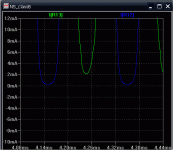
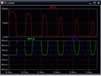
It still has a problem. Even as this was only reproduced on a simulator , I use the NJL-xxxx's and MJE's all the time and the models a VERY close to the real world. In the attached graph , the first ms of signal switches different than 3 or more ms into the sim.
Otherwise , I ran the optimized OP stage (attached schema- R2 might be a VR) with a standard self VAS/ typical LTP w/NFB , and the resulting amp was <.01thd any freq. Switching did not occur until 20v-pp and the Xover point remained constant.
BTW , any ideas on how to port this to a fully complimentary version , I'm slightly befuddled ???
OS
Attachments
Yes at frequency=const the rise time of a sine signal around zero is proportional to the amplitude. However what is the stringent reason for a complementary design?
In a standard class AB it is obvious that 2nd order distortion is reduced. I am not sure whether this applies to this topology.
In a standard class AB it is obvious that 2nd order distortion is reduced. I am not sure whether this applies to this topology.
Pete,
I will look at the complementary version. I'm having some issues with the negative half cycle current limiting, but it looks dooable. As a general rule, complementary output stages reduce THD, but only the musical evens, not the odds. You have to ask why you bother, a quasi can sound VERY good indeed. Of course, if your goal is very low THD, go for it.....
The outputs definitely switch, but the crossover is immaculate, really clean. I'm not sure that switching needs to be a problem if crossover is really well handled.
Hugh
- Status
- This old topic is closed. If you want to reopen this topic, contact a moderator using the "Report Post" button.
- Home
- Amplifiers
- Solid State
- Class B w/o crossover distortion (1975)