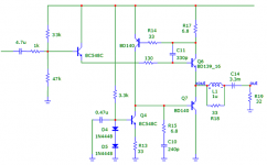
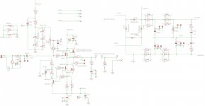
If you're about mine schema - 220pF is not enough to compensate load's capacitance so add damped inductance before output. I made inductance as ~10 windings of D=1mm wire on D=1cm carcass. How it looks on circuit with such output stage (but with diffrent input) is attached as prototype_outview.jpg. May be simple ferrite bead instead will be good too if have enough inductance.
And if you're using 2-stages follower its can be useful to add few other corrections, see another attached pic.
And if you're using 2-stages follower its can be useful to add few other corrections, see another attached pic.
Attachments
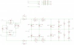
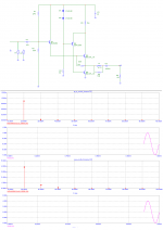
I don't think that a pure sine makes a particularly good model for your buffer's power draw. I'd also say that looking at the supply while delivering sizeable output power is only step 2. First you'd be looking at idle, where load current draw is constant.I simmed a rcrcrc supply, +ve rail only, pics with 20hz and 20khz load and asc file are attached.
As for load modeling in step 2, I would expect:
positive supply - constant current with a varying amount of signal (e.g. sine) riding on top
negative supply - constant current
So if anything, you'd need two parallel current sources to simulate +Vs loading.
Of course delivering output power will cause increased supply ripple, but thanks to PSRR this shouldn't do anything too bad (except decrease clipping levels, of course - see power bandwidth). In a Class A circuit like this there pretty much isn't any distorted crap riding on the supplies like there would be in a switching (B/AB) amplifier, so you can get good results even with moderate amounts of PSRR. The bit of extra distortion that will be generated should be a result of Early voltage and input capacitance nonlinearity effects. (Distortion may even cancel in very specific case though, namely if supply ripple becomes just as large and in phase with input voltage.)
Design your PSU+Amp to have adequate ripple rejection.
test with a quiescent DC load current.
Is it 500mAdc or 1Adc?
Get the amp to work with what is left as a quiescent ripple. That is when you are going to hear it worst (no signal condition).
Then think about where the amp gets it's signal current from.
It initially comes from the last capacitor. Get that capacitor big enough to supply the demands of the amplifier. The preceding parts of the PSU re-charge that cap as best they can and try to minimise the supply rail droop when demand is high.
Remember that the fastest changes in current demand are met by the on board local decoupling capacitors.
The load I specified in the previous images is SINE(0.5 0.25 20), where the 0.5 is the dc offset, 0.25 is the amplitude of ac in amps and 20 is the frequency in hz. I guess thats why the confusion arose as I didnt create two separate parallel loads for ac and dc. I checked the current waveform and its correct.
I tested it with only 500mA DC load also for Iq testing. I get about <2mv ripple. There is also diode noise. It goes away if I replace the diodes and ac supply with DC, and it also gets reduce d if I put 0.1uf caps across the diodes.
I didnt test the -ve supply so far, I presume it will give the same results as +ve with 500ma DC.
I will put both the supply rails sims into the amp sim and see how much of the ripple is left at the output.
Last cap is 10kuf. On board the amp, i will have a 4700uf cap per rail per channel. The first cap is 4700uf and has low esr (about 22 mohm).
Last edited:
The mains ripple is down to <2mVac with a DC load of 500mAdc. That's good.
This will increase if you increase the load current.
Applying an AC load will modulate the supply rail voltage. That is NOT mains ripple. That is the natural/inherent output impedance of the supply times the AC current.
This will increase if you increase the load current.
Applying an AC load will modulate the supply rail voltage. That is NOT mains ripple. That is the natural/inherent output impedance of the supply times the AC current.
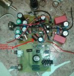
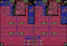
psu pics... big caps are 25mm.
I am doing breadboarding of the amp today (with a lm317/337 supply that i already have). I have made only one channel and would be trying with some cheapo headphones... how do I connect both channels of the headphones to the single channel amp. Sound quality in a single spkr working in the ears is kinda difficult to make out.
I am doing breadboarding of the amp today (with a lm317/337 supply that i already have). I have made only one channel and would be trying with some cheapo headphones... how do I connect both channels of the headphones to the single channel amp. Sound quality in a single spkr working in the ears is kinda difficult to make out.
Attachments
Got it, will tr with some small resistor (0.5R) in series with both the loads.how do I connect both channels of the headphones to the single channel amp.
Hi,
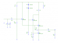
You may omit with R4. R5 has negligible impact and may be raised to 1k.
C3 should be a bipolar cap.
optional:
- You may split R1 in two resistors with increased value (5K-10k) and add a cap of a few µF from the resistor mid-joint to the negative supply.
- You can omit with the output coupling caps using a active DC-servo that controls the idle current of the ccs, and a bias voltage and a source resistor for the MOSFET.
For an example of the servo circuit see my website calvins-audio-page.jimdo.com/ideas-and-circuits/buffers/hybrid-buffer-en/.
Scroll down to "Calvin-Buffer plus dc-servo".
jauu
Calvin
Hi, Calvin
I checked out your site but couldnt find that servo, however I came across your page on BJT buffers and something stuck out.
Regarding emitter followers you mention :
''As can be seen in the pictures, the circuit works with a single supply voltage, but can also be used with a dual symmetrical operating voltage. With good transistor matching and clean adjustment, the output capacitor can then be dispensed with.''
I did not think this was possible for EF circuit without a servo, and this is exactly why I am searching for servo.
Would you mind elaborating more on that circuit, an EF without output coupling cap?
Excuse me for diggin this one out but it simulates nice enough and I´m looking to eventually build it for ~1W output...yet another class A buffer idea (didn't test in HW yet)
Did you ever try the design? Might give this (blindly) a try.
- Home
- Amplifiers
- Headphone Systems
- class A Buffer