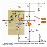
The schematic in post 127 was what I posted based on the Danyuk article cited by 00940, to which Shaq basically said it was wrong.
He didn't say it was wrong. He questioned whether connecting the feedback network to an opamp that's connected to the non-bootstrapped supply defeated the purpose of the circuit in the first place (connection marked in blue). He further elaborated that the low impedance of the feedback network (200||1800 Ω) probably saved the circuit.
I agree with this assessment. The purpose of the circuit is to bootstrap the input capacitance of the LME49710. According to the author, this capacitance causes a nonlinear current to flow in the input circuit, which increases the distortion. If this is true, then the bootstrapping opamp (U2) should have the same nonlinear current flowing in its inputs as it is seeing the same voltage swing as the bootstrapped input (U1). This nonlinear current is added to the feedback currents in the first opamp, which adds distortion to the output of U1. The saving grace may be that the nonlinear current cannot generate much error voltage across the feedback network due to its low impedance (200||1800 Ω).
Also note that the circuit is intended for use with high-Z sources (1 MΩ source impedance). This is hardly applicable in the audio world. What I'm suggesting is to try the other tricks mentioned in the first few paragraphs of the article. We discussed one of those tricks (balancing the impedances 'seen' by the inverting and non-inverting inputs of the opamp) in this thread just a few days ago. You didn't seem terribly interested in that idea then.
So, I am not smart enough to understand what part of the schematic to keep or change. Again, a schematic of what Shaq actually has in mind would be helpful.
I agree that a schematic would be nice, but as Shaq has explained already, he's accessing DIY Audio from a phone most of the time and at the time of your request for a schematic didn't have anything available to draw on so he could take a picture to post. You can't expect that people serve everything to you on a silver platter and I doubt you improve your chances by questioning his computer skills. In addition, you seem to gloss over much of the information you're given, which further reduces your chances.
I will read it again, it’s enjoyable as it comes with schematics.
Yes it does. But sometimes you can get more information if you read the text in addition to looking at the pictures.
There's an ambiguity in the schematic by the way. I've added a solder dot in red.
Tom
Attachments
Hi Tom,
Where does the other end of R8 go?
-Chris
To the driven guard ring/shield if my brain hasn't failed me (not a guarantee at all!!!!)
Also note that the circuit is intended for use with high-Z sources (1 MΩ source impedance).
BTW, in case of such a high impedance of a source 49710 may not to be a rational choice due to relatively high current noise.
What about a sketch with pencil and paper and post a photo?
That wasn't available at the time. This was mentioned in the post.
BTW, in case of such a high impedance of a source 49710 may not to be a rational choice due to relatively high current noise.
I agree. A low Ib opamp would be a better choice.
Tom
Sooo, why not just ground the shield? It's not like you're driving the shield on a triax high Z connection.
The assumption is probably that the leakage through the board is nonlinear. Hence, the author bootstrapped those leakage caps as well.
Whether this assumption is valid is another thing. I'd certainly welcome a measurement of with/without R8. Or shield driven vs shield grounded.
Tom
I "extrapolated" the data a have for the 1688 and was trying to compare it to 1642 and I got stuck since I can not find a good common mode distortion plot for the 1642. The appnote you posted earlier does not state signal magnitude. If it is around 1Vrms than 1642 is not clearly better in that respect. Although it is hard to say for sure, they seem to be masked by other types of distortion.
Last edited:
No, indeed no plot for common mode distortion in isolation. Still the app note gives a flat common mode capacitance for a common mode voltage from -10 to +10v
Edit: there is this too http://www.diyaudio.com/forums/vendor-s-bazaar/283672-audio-op-amp-opa1622-9.html#post4636374
Edit: there is this too http://www.diyaudio.com/forums/vendor-s-bazaar/283672-audio-op-amp-opa1622-9.html#post4636374
Last edited:
Hi Tom,
Certainly possible. But in that case all you would need is a guard ring in foil on all layers. You would need that anyway just for an effective shield. Physical space from other conductors would be the best first choice, but a driven ring & shield would allow a much smaller PCB. The shield would need a warning label mentioning that it is live and not grounded!
Now the question is, where do you couple the supplies to a "dirty" ground for shields? That would have to happen right at the op amp driving the shield to keep signals it picks up away from the circuit. I see it is a single package (good), but I don't think it needs to be an LME49710 to do it's job. Nice but not critical, an NE 5534 could probably do. I agree with Shaq888 that it should have it's signal supplied by it's own divider chain no matter what the op amp is.
-Chris
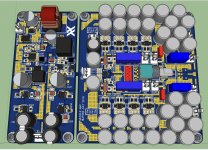
I made a simple experiment where I repurposed one opamp from the output bunch for the bootstrapping. As expected, works without any problems. Clipping looks OK. Of course it reduces output power handling, but not by a huge lot. Beside that I see no problems in creating two PCB loading variants. By fitting corresponding resistors that opamp can be connected to the output to maximize output power or it can be used for bootstrapping if it is more important. PCB area increase should be pretty minimal.
Added supply bootstrap to my old design - "The Crocodile"
Also have thrown in a relay and hooked it up to a startup delay/DC protection/brownout detector.
As before there is a switch mode PS on board that would work from single Li-ion cell (with limited power) up to 12-ish volts.
Amplifier can be configured as inverting, balanced or non-inverting with bootstrapped power supply if needed.
PCB is approx 50x70mm.
Will put gerber files and BOM somewhere for public access after I finish, so anyone who wants can order them (PCBway of Seeedstudio are your best friends in this case).
Now it looks like this:
Added supply bootstrap to my old design - "The Crocodile"
Also have thrown in a relay and hooked it up to a startup delay/DC protection/brownout detector.
As before there is a switch mode PS on board that would work from single Li-ion cell (with limited power) up to 12-ish volts.
Amplifier can be configured as inverting, balanced or non-inverting with bootstrapped power supply if needed.
PCB is approx 50x70mm.
Will put gerber files and BOM somewhere for public access after I finish, so anyone who wants can order them (PCBway of Seeedstudio are your best friends in this case).
Now it looks like this:
Looks nice! Always like the composite amplifier designs.
That's funny and sad simultaneously to see all those efforts are wasted by a few basic mistakes. Too bad you never get to making any better measurements that you did. It could help you to avoid making those.
That’s quite impressive that you can spot mistakes on a new OPA1622 buffer amp design and layout without seeing the schematic as that was not posted. Thanks for your suggestions, and I would perhaps have implemented them, if you had shown more details and a schematic of what changes you suggested.
I think the design I have now achieves its goals, and kindly suggest that you start your own thread for further discussions of your ideas on improving the circuit.
- Status
- This old topic is closed. If you want to reopen this topic, contact a moderator using the "Report Post" button.
- Home
- Amplifiers
- Headphone Systems
- Cheap as Chips OPA1688 Low-THD Muscle Amp