Wow, there's a lot of posts to plough through here!
I didn't do any Vgs matching before I built the circuit (he says sheepishly) In fact, It's not something I've ever even tried, so I'll have to work out how to do it.
I've shortened down my test leads and re-arranged my bench accordingly.
I'm working on measuring all the currents and marking them on the diagram.
We're on the flattest part of the 1381 GBP curve at 2 to 5mA, so somewhere around 140 to 150MHz.
The buz datasheet doesn't show anything analageous to the GBP data for the 1381/3503 though. Input and output capacitance are show as 500 and 300pf @ 1MHz, however, which compares to the 1381 Cob of 2.6pf @ 1MHz
I can't remember why I came up with the r10 value at 47r. I remember thinking about it, but it's not in my notes. I'll amend accordingly.
The pots to vary the current for VAS and LTP are there out of curiousity. I wanted to be able to see what happens when it's adjusted. A good point well made about knowing what the actual currents are though. The answer is I build them first, then measure and mark.
Elvee, thanks for the simulations. I'll try the resistors in due couse.
I did do a bit of research when I was putting it together, but I didn't find much on the actual design of this OP topology, so I thought I'd give it a go to try and learn about it. Self more or less dismisses fets, and Slone seems to have made some weird design decisions, although he uses this configuration quite a bit. The art of electronics has very scant infomation in this area too, and I couldn't find much elsewhere, so I put something together and started investigating.
Fundamentally, Andrew is right, it is a bit banged together, but simply because I had the fets, and it's something I wanted to investigate, rather than a desire to have a working circuit straight away. I had no idea how difficult this particular approach would be, and It's pretty clear that I've got a lot to learn, but that's why I'm here I really do appreciate all the help, and I hope the thread ends up as a good resource for anyone considering something similar.
I'll keep you posted on progress
I didn't do any Vgs matching before I built the circuit (he says sheepishly) In fact, It's not something I've ever even tried, so I'll have to work out how to do it.
I've shortened down my test leads and re-arranged my bench accordingly.
I'm working on measuring all the currents and marking them on the diagram.
We're on the flattest part of the 1381 GBP curve at 2 to 5mA, so somewhere around 140 to 150MHz.
The buz datasheet doesn't show anything analageous to the GBP data for the 1381/3503 though. Input and output capacitance are show as 500 and 300pf @ 1MHz, however, which compares to the 1381 Cob of 2.6pf @ 1MHz
I can't remember why I came up with the r10 value at 47r. I remember thinking about it, but it's not in my notes. I'll amend accordingly.
The pots to vary the current for VAS and LTP are there out of curiousity. I wanted to be able to see what happens when it's adjusted. A good point well made about knowing what the actual currents are though. The answer is I build them first, then measure and mark.
Elvee, thanks for the simulations. I'll try the resistors in due couse.
I did do a bit of research when I was putting it together, but I didn't find much on the actual design of this OP topology, so I thought I'd give it a go to try and learn about it. Self more or less dismisses fets, and Slone seems to have made some weird design decisions, although he uses this configuration quite a bit. The art of electronics has very scant infomation in this area too, and I couldn't find much elsewhere, so I put something together and started investigating.
Fundamentally, Andrew is right, it is a bit banged together, but simply because I had the fets, and it's something I wanted to investigate, rather than a desire to have a working circuit straight away. I had no idea how difficult this particular approach would be, and It's pretty clear that I've got a lot to learn, but that's why I'm here
I really do appreciate all the help, and I hope the thread ends up as a good resource for anyone considering something similar.I'll keep you posted on progress
Hi ian_elvar
Some of your problem is with the actual dual die devices.
I have had a lot of experience with these devices.
The dies them selfs have no internal gate resistors.
The dies are simply connected in parallel and bonding wires
connected between them.
Unlike the Hitachi single die laterals that actual have a 30 ohm resistor etched into the die gate.
One of the best ways of lowering the lead inductance and therefore helping to stablize these devices is to bolt them directly down to a large heat sink without insulators. But this cannot be done in your case because of the common drain output. If you have access to some single die hitachi or renesas devices, try them first to prove your design.
I agree with Eva, put a zobel network on the output of this amplifier and use a 10 ohm 5 watt in series with a 100nf capacitor as a good starting point.
Do not try and work it without doing this.
I have designed and built 2kw amplifiers using these dual die devices and zobel networks are a must do.
I hope this helps
ian,
the CFP has many remarkable features. Being a closed-loop there is always risk of oscillation, things may not work right away but the results justify the pains. The devices used have indeed explicitly appropriate properties to succeed. I cannot see anything wrong with BUZ901D nor the very important driver. (I use to heavily criticize people when choosing unsuitable types for voltage amplification). 2SC3503/2SA1381(100MHZ@5mA, 160MHz@10mA, 200MHz@30mA) are nice, although there are faster types like 2SA3600/2SA1406 (200MHz@5mA, 300Mhz@10mA, 400MHz@30mA) with excellent linearity.
Please look at this one for some details of relevance.
http://www.diyaudio.com/forums/showthread.php?s=&threadid=119151
Eva,
the CFP has many remarkable features. Being a closed-loop there is always risk of oscillation, things may not work right away but the results justify the pains. The devices used have indeed explicitly appropriate properties to succeed. I cannot see anything wrong with BUZ901D nor the very important driver. (I use to heavily criticize people when choosing unsuitable types for voltage amplification). 2SC3503/2SA1381(100MHZ@5mA, 160MHz@10mA, 200MHz@30mA) are nice, although there are faster types like 2SA3600/2SA1406 (200MHz@5mA, 300Mhz@10mA, 400MHz@30mA) with excellent linearity.
They lower the feedback. It would be important to achieve stability in a not too harmful way, i. e. limiting the bandwidth, using nonlinear parts. Hugh´s proposal extends the bandwidth and linearizes the drivers as decreasing the gain.what does AKSA's 10r to 22r in the emitter lead do for the oscillation?
Please look at this one for some details of relevance.
http://www.diyaudio.com/forums/showthread.php?s=&threadid=119151
Eva,
He has: 5MHzI think you have not mentioned the oscillation
frequency.
Eva - I'm still using the first PCB that I put in the first post, although slightly modified (cut tracks to rectify VR3/C8 mess, and add in emitter resistors at Elvee's suggestion). Oscillation is indeed 5MHz.
Would you mind going into slightly more detail about what you think is wrong with supply layout and decoupling, so I can start researching how to improve it? I'm happy to make another PCB, it's really not a problem. Current layouts are attached.
Anthony - Thanks for your comments. The Zobel is currently implemented, and as it happens I do have an old pair of working Hitachi J50 and K135's, so I'll pop them into the circuit for the moment.
Lumba - By nonlinear components I assume you mean in this case something that increases resitance at higher frequencies?
Thanks for the hints on other transistor types. I think it might have been you that put me on to the 1381/3503 pair a little while back.
Updated diagrams:
An externally hosted image should be here but it was not working when we last tested it.
An externally hosted image should be here but it was not working when we last tested it.
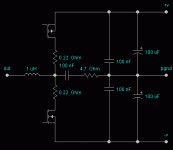
The output section should resemble this picture, both as a schematic and as a PCB layout.
Common practices such as placing the decoupling capacitors away from the output transistors or routing the supply rails through the sides of the PCB and placing the small signal circuits in the center are completely wrong. Placing the power ground connection in the opposite side of the output stage is also a bad idea. The current loops that matter are the ones involving speaker current and their area should be minimized. These tracks should be wide too (and short), not due to current requirements but because inductance increases dramatically as thickness is reduced. On the other hand, inductance in small signal layouts is almost irrelevant.
You may consider a double sided PCB with a continuous ground plane on the top side to further reduce parasitic inductances (it acts as a "shorted turn").
The problem with CFP and MOSFET is that they exhibit gain up to quite high frequencies where common layout practices are not good enough. You can expect high "gain" up to at least 50Mhz from your output devices.
Attachments
Eva said:The output section should resemble this picture, both as a schematic and as a PCB layout.
Common practices such as placing the decoupling capacitors away from the output transistors or routing the supply rails through the sides of the PCB and placing the small signal circuits in the center are completely wrong.
Eva,
How do you propose routing the power traces then, both V+ and V- running along one side of a double sided PCB? Bringing small signal in from the other side?
Could you draw a picture?
Thanks,
Scott
The current state of affairs:......
I have the circuit in front of me running a 30V peak to peak 10KHz square wave with no sign of oscillation. The bais behaves as it should, clipping doesn't create any nasties, and the bias current is staying stable. It's happy having the supply rails altered too, although my bench supply only does +/- 30V maximum. Some progress has clearly been made!
Eva - Thanks for the layout hints, I'll see what I can come up with. If you wouldn't mind drawing a quick sketch it would be most helpful. Any suggestions for further reading on the matter?
Unclejed - VAS overload protection is Q14's purpose. I found with simulation that you can easily draw waaaaay too much current on the negative swings through the VAS by driving a circuit of this configuration into clipping if it isn't fitted. C1 being the compensation capacitor is connected to the base of Q3.
I have just spotted a couple of mistakes on the schematic though - Q14 is not a 2SC3503, it's a 2SC1775. Also I've forgotten to show R36 as jumpered at the moment. R10 has been brought down to 18r. I still can't figure out why I made it 47!
I think I'll try lowering the base stopper resistors now to see what happens. I have a feeling that with the 'Elvee' resistors installed it should now be better behaved.
Ian,
Well done. That sounds like progress. What did you change between this post and the one before, where you still had oscillation?
After you have updated the schematic again (please put the zobel in and all the component values, and anything else you may have added, thx), would you mind measuring the dc voltage across R22 and the dc voltage across R23?
More still to do.
Brian
Ian,
Very good but...
I`m not quite happy with the output biasing and phase compensation technique. Please take a look at Karl`s design for inspiration. The open-loop gain is too high to my taste.
traderbam,
Very good but...
I`m not quite happy with the output biasing and phase compensation technique. Please take a look at Karl`s design for inspiration. The open-loop gain is too high to my taste.
traderbam,
Inserted R37/R38.What did you change between this post and the one before, where you still had oscillation?
Lumba Ogir said:Ian,
Very good but...
I`m not quite happy with the output biasing and phase compensation technique. Please take a look at Karl`s design for inspiration. The open-loop gain is too high to my taste.
traderbam,
Inserted R37/R38.
Yes, the dynamic behaviour is suspect. One step at a time.
I was confused by post #45, where Ian says the oscillation is 5MHz and also shows the schematic with those driver emitter resistors in place. Perhaps he meant the oscillation was previously 5MHz.
I think Ian has made these changes so far:
1. Shortened and bundled the psu wires
2. Corrected the bias circuit decoupler
3. shorted R36
4. Added an RF filter to the input
5. Reduced R10 to 18 ohms
6. Reduced R22/R23 to 220 ohms
7. Changed the gate resistors to 470 ohms and removed the ferrite beads
8. Added R37/R38 of value 22 ohms
Have I missed anything?
0.5 V across R23, and 0.8V across R22
Supply rails are +/- 30V
Bias is set to 1.35V C-E of Q7, and each rail is drawing about 50mA at idle.
DC offset could be worse at 10mV
I think it was adding R37/38 and correcting C8s position that sorted out the parasitic and bias problems respectively. The other stuff was all common sense that managed to pass me by. For example, forgetting to short R36 would result in some really rather nasty negative clipping behaviour. Lowering the value of R10 then smoothed things out totally, and it now clips very gracefully without complaint. It would take a while to recover before, whilst oscillating and drawing way more current than it should. Who knows what will happen when I un-short it, and put some caps in though...
I do still need to add better filtering at the input, and measure a whole load more voltages around the circuit. It does seem to be picking up some crud along the way. When the circuit is powered up and input shorted I can see a messy sine wave 30mV pk2pk@50KHz on the trace. It's exactly the same frequency that appears if I take the probe off and touch my finger to the end, and the amplitude varies greatly if I put a finger near the input caps, particularly on the copper side.. Something that needs attending to rather urgently!
An updated schematic and layout:
I've marked where the ground connections back to the star point are, in case it wasn't clear before. No-one else normally looks at my PCB layouts or schematics (well, only people that think they're some kind or modern art or computer graffiti!), so I've slipped into some bad habbits not labelling things properly because I know what they're meant to be. I've just noticed that I still haven't marked on a few cap values, but it will have to wait till tomorrow as I need to go to bed!
An externally hosted image should be here but it was not working when we last tested it.
An externally hosted image should be here but it was not working when we last tested it.
Lumba Ogir said:Ian,
Very good but...
I`m not quite happy with the output biasing and phase compensation technique. Please take a look at Karl`s design for inspiration. The open-loop gain is too high to my taste.
traderbam,
Inserted R37/R38.
Do you mean using a plain resistor, rather than a VBE multiplier? I take it you mean global OL gain?
traderbam said:
Yes, the dynamic behaviour is suspect. One step at a time.
I was confused by post #45, where Ian says the oscillation is 5MHz and also shows the schematic with those driver emitter resistors in place. Perhaps he meant the oscillation was previously 5MHz.
I think Ian has made these changes so far:
1. Shortened and bundled the psu wires
2. Corrected the bias circuit decoupler
3. shorted R36
4. Added an RF filter to the input
5. Reduced R10 to 18 ohms
6. Reduced R22/R23 to 220 ohms
7. Changed the gate resistors to 470 ohms and removed the ferrite beads
8. Added R37/R38 of value 22 ohms
Have I missed anything?
Yes, I referring to previously when the oscillation was 5MHz
All other points correct apart from:
4: Not done yet. Next on my list!
7: Still 1K5 at the moment - will experiment more in the morning.
Good stuff, Ian.
More essentials...
A 500pF or so cap from pin 7 of IC1 to ground is very important, not just to reduce RF at the input but also to reduce instability associated with the input stage.
Also to improve stability, increase R1 to 1k and make R1 and R4 in the region of 33k. This will reduce the amp's gain a little too.
I've had a study of your output transistors. They still aren't stable enough at high currents for my liking, nor are they balanced due to the significantly different capacitances of the N and P channel FETS. To improve this situation I recommend making R38 and R37 33 ohms. Make R26 1k and R27 2.2k. Keep R22 and R23 at 220 ohms.
I cannot simulate your circuit accurately because I don't have the models for your transistors, nor do I have the time.") So I would strongly recommend you take the precaution of adding a network at the output in series with the speaker wire. A 2uH (or close) inductor in parallel with a 10-ohm resistor. This helps reduce the capacitive phase shifts of the speaker and speaker cable from destabilizing the output stage.
So I would strongly recommend you take the precaution of adding a network at the output in series with the speaker wire. A 2uH (or close) inductor in parallel with a 10-ohm resistor. This helps reduce the capacitive phase shifts of the speaker and speaker cable from destabilizing the output stage.
Once you are happy with the basic circuit, do your bench tests and make sure it is behaving itself. Aside from checking it can make a sinewave at full swing without visible problems, both loaded and unloaded, it is important that there is no mains hum appearing at the output and that there is no high frequency fuzz or other discernable patterns. You should only see random noise. What test equipment have you got? Is your scope analogue or digital  ?
?
Then hook it up to a speaker and listen to it (and watch it on a scope at the same time)! See how good it sounds.
If you are still keen after all that, there are a few more circuit changes you can make that will improve its sound quality. Such as the psu decoupling on the pcb, cranking the NFB up and dealing with those pesky SSM ICs. Not to mention a myriad of good ideas from everyone else. One step at a time.
Brian
More essentials...
A 500pF or so cap from pin 7 of IC1 to ground is very important, not just to reduce RF at the input but also to reduce instability associated with the input stage.
Also to improve stability, increase R1 to 1k and make R1 and R4 in the region of 33k. This will reduce the amp's gain a little too.
I've had a study of your output transistors. They still aren't stable enough at high currents for my liking, nor are they balanced due to the significantly different capacitances of the N and P channel FETS. To improve this situation I recommend making R38 and R37 33 ohms. Make R26 1k and R27 2.2k. Keep R22 and R23 at 220 ohms.
I cannot simulate your circuit accurately because I don't have the models for your transistors, nor do I have the time.
So I would strongly recommend you take the precaution of adding a network at the output in series with the speaker wire. A 2uH (or close) inductor in parallel with a 10-ohm resistor. This helps reduce the capacitive phase shifts of the speaker and speaker cable from destabilizing the output stage.Once you are happy with the basic circuit, do your bench tests and make sure it is behaving itself. Aside from checking it can make a sinewave at full swing without visible problems, both loaded and unloaded, it is important that there is no mains hum appearing at the output and that there is no high frequency fuzz or other discernable patterns. You should only see random noise. What test equipment have you got? Is your scope analogue
or digital ?Then hook it up to a speaker and listen to it (and watch it on a scope at the same time)! See how good it sounds.
If you are still keen after all that, there are a few more circuit changes you can make that will improve its sound quality. Such as the psu decoupling on the pcb, cranking the NFB up and dealing with those pesky SSM ICs. Not to mention a myriad of good ideas from everyone else. One step at a time.
Brian
Ian,
Yes, and a polypropylene capacitor in parallel, there is no need for a VBE multiplier here.Do you mean using a plain resistor, rather than a VBE multiplier?
traderbam said:Good stuff, Ian.
More essentials...
A 500pF or so cap from pin 7 of IC1 to ground is very important, not just to reduce RF at the input but also to reduce instability associated with the input stage.
Ok, that sounds sensible.
traderbam said:
Also to improve stability, increase R1 to 1k and make R1 and R4 in the region of 33k. This will reduce the amp's gain a little too.
I take it you mean R3 to 1K? Yes, the CL gain is a little unconventionally high at the moment. It will be a little noisier with higher value resistors, but in this case I think that's an acceptable trade for stability. How does it help though?
traderbam said:
I've had a study of your output transistors. They still aren't stable enough at high currents for my liking, nor are they balanced due to the significantly different capacitances of the N and P channel FETS. To improve this situation I recommend making R38 and R37 33 ohms.
Ok, so you're suggesting cutting down a bit more of the feedback. We're getting away from the value that AKSA and Elvee and suggested from his simulation though, so I'll try to run it myself
traderbam said:
Make R26 1k and R27 2.2k. Keep R22 and R23 at 220 ohms.
I agree, it makes sense to keep the driver current where it is. Do you not mean R27 1K and R26 2K2 though? The 906D has double the capacitance of the 901D, so surely it makes sense to put the larger cap on the 906D gate? Or am I missing something?
traderbam said:
I cannot simulate your circuit accurately because I don't have the models for your transistors, nor do I have the time.
There will be an output network, but it's off board on the DC protection PCB.
traderbam said:
Once you are happy with the basic circuit, do your bench tests and make sure it is behaving itself. Aside from checking it can make a sinewave at full swing without visible problems, both loaded and unloaded, it is important that there is no mains hum appearing at the output and that there is no high frequency fuzz or other discernable patterns. You should only see random noise. What test equipment have you got? Is your scope analogue
I have an ISO-TECH 20MHz analogue scope, an old Marconi TF2331 distortion meter (not a particularly sensitive instrument though), and an HP3580A spectrum analyser. Once I've got the circuit in better shape I'll try testing it with a dummy load and take it from there. It's certainly well behaved just wiggling a voltage into the air though.
traderbam said:
If you are still keen after all that, there are a few more circuit changes you can make that will improve its sound quality. Such as the psu decoupling on the pcb, cranking the NFB up and dealing with those pesky SSM ICs. Not to mention a myriad of good ideas from everyone else. One step at a time.
Brian
Yes, it's quite hard to keep up! If it's looking promising I'll make a final schematic and start designing a better PCB
Eva said:If you have any compact fluorescent lamp (or one with an electronic ballast) close to your workbench, it may be the source of the 50Khz stuff.
Spot on. It was the energy saving bulb in my angle poise bench lamp.
- Status
- This old topic is closed. If you want to reopen this topic, contact a moderator using the "Report Post" button.
- Home
- Amplifiers
- Solid State
- CFP oscillation woes