
the current DIFFERENCE bewteen the two bases of the input transistors should be near zero.
It appears that there is something wrong with the current difference. That points to one, or other, of the input transistors passing an excessive current.
The 10r showing a high DC voltage between Signal Return and Decoupling Ground pointed the finger.
Could there be leakage current through the decoupling capacitors that are connected to the Signal Return?
@Sherlock Holmes ")
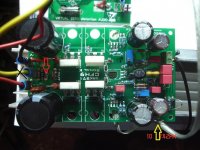
In past at input for a bridged Sansui power amp i also used sockets as in picture so as to switch between components and remember it gave me trouble at some time where zobel resistors burned and also in general there was degraded sound quality compared to when components was real soldered.
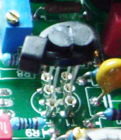
In past at input for a bridged Sansui power amp i also used sockets as in picture so as to switch between components and remember it gave me trouble at some time where zobel resistors burned and also in general there was degraded sound quality compared to when components was real soldered.


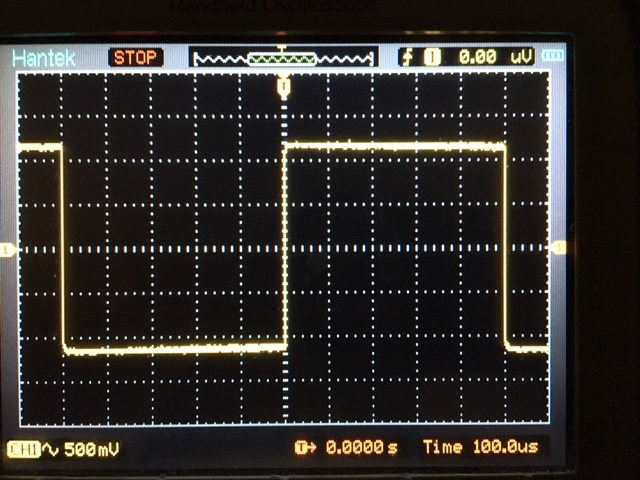
I just wanted to remind folks that back on post 438, I got some pretty clean O-scope traces of a square wave. I borrowed a friend's DSO so do not have it now but don't recall all the noise.
Closeup:
I hope you find the @#$%!@#$*!!@ B@stard
It does remind me of a similar thing I went through when we were debugging the Aksa/Ranchu Quasi MOSFET amp. That one took some blood from me
Closeup:
I hope you find the @#$%!@#$*!!@ B@stard
It does remind me of a similar thing I went through when we were debugging the Aksa/Ranchu Quasi MOSFET amp. That one took some blood from me
Last edited:
I will find the bastard.
I promise.
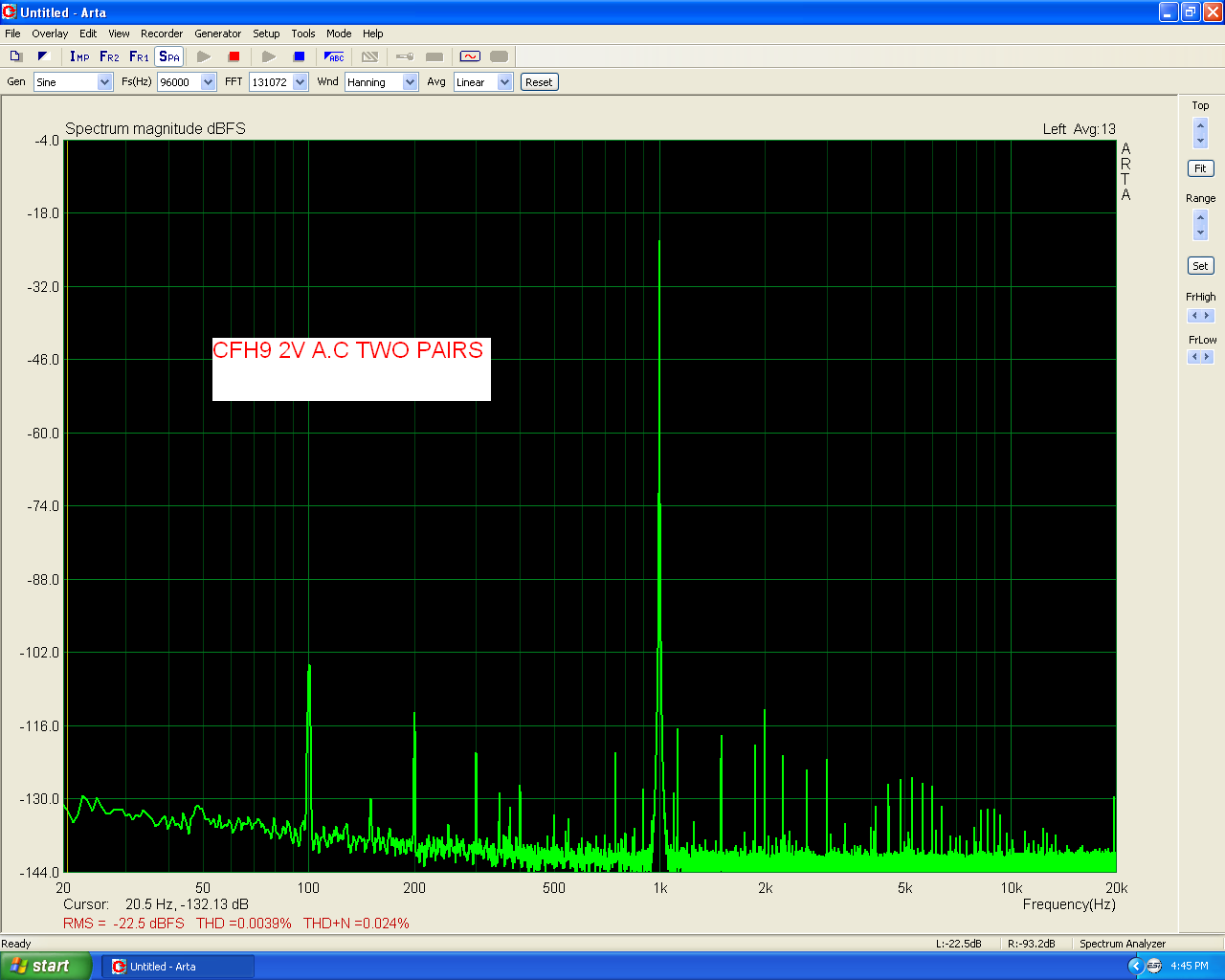
Ricky this amplifier is stable,tested without any zobel,tested with 100nf+10R1/4 Watt as zobel to see if this will burned . Nothing happen even at 50 Khz 17V Square wave output.
I will find the bastard
Great, sound you in mood to nail it soon will .....

I will do the CFH9 like thisGreat, sound you in mood to nail it soon will .....
Attachments


Ok boys,bastard is dead i hope..
So what exactly was the reason of these problems?
I will triple check and i will report soonSo what exactly was the reason of these problems?

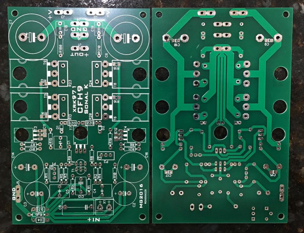
CFH9
This power GND completely removed!
Please Keep in mind that there are some other modifications and i will try to find if it is necessary or not.
I had tried the same in the past but without success because i had keep the ground connection for the two input filter electrolytics.
This power GND completely removed!
Please Keep in mind that there are some other modifications and i will try to find if it is necessary or not.
I had tried the same in the past but without success because i had keep the ground connection for the two input filter electrolytics.
Attachments
Last edited:
This power GND completely removed!...
If that did and i have read it right then C7 bypassed C9 and C6 bypassed C10 filter and store from rail to rail instead so either of those capacitors maybe is faulty as shaan was into as e seldom fault.
Well lets see later on, but great you had big progress
Interesting. The two series caps are now simulating a half-sized cap from plus to minus, almost like what is standard in opamp designs.
I like this amplifier very much but I have a few questions regarding the layout.
Why are the power rail decoupling electrolytics so big? These are not reservoirs; their purpose here is to shunt any abnormal activity in the rails to ground. For this purpose even a 100uF is sufficient and will cause less problem in transient production than the inductance of the speaker cable itself.
Why are the main current carrying power traces emerging from their entry points alone without an accompanying ground trace, especially when the first thing they meet is a bunch of trigger-happy hexfets? Two close-by traces always develop very small stray capacitance between them and this prevents the power rails from acting like antenna and makes decoupling semiconductors far from power input very easy.
Must one use parallel small caps? I have tested this kind of amps with 100KHz 16nS risetime squarewaves at 40VPP without ANY film caps in the rails and they do not show any form of misbehavior. IMO these small caps are plain unnecessary in this amp, as thimios's previous tests showed. If you have to use them, then install them as close as possible to the semiconductors(where they will actually do some work), not under the electros. I won't comment on using them with the feedback capacitors as it seems to me now as a matter of taste.
The two zobels make the power side look very good! But they should be terminated to the ground through their own traces to prevent interference between them and any other stabilizing components i.e. the huge electrolytics.
..................................................
Now, I will try to explain why both input and feedback can not be grounded through a lift resistor as much as I understand it.
If a lift resistor is used then for any given input signal the AC feedback current (which also flows through the lift resistor) will be equal to the Ratio of the input bias resistor and the feedback resistor multiplied by AC input current through the input bias resistor. In this case it is 22000/47=468 times the AC current through the 22K resistor.
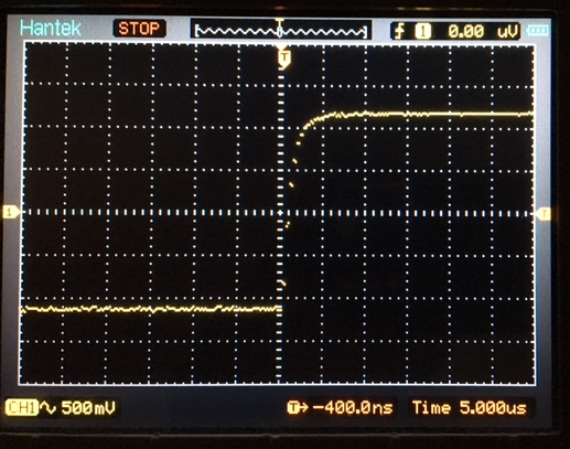
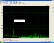
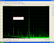
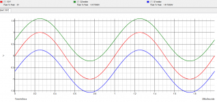
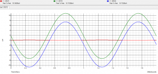
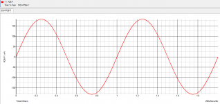
See the first picture. It shows input voltage (red) and the two feedback voltages (green,blue) at each input BJT's emitters. Naturally the feedback voltages are off-set from 0V, but their amplitude seem almost same as input voltage of ~2VPP. Now look at the second picture. It shows AC current through the input bias resistor (10K in this case)(red) and the two feedback resistors (100R in this case)(green,blue). And the feedback current is 100 times higher in amplitude (10K/100R).
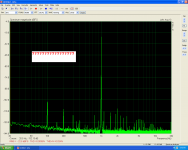
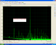
The result is summing of the input and feedback current and the resultant AC current flows through the lift resistor which will present an AC voltage in the input cable shield instead of a clean ground! Now imagine connecting two amplifiers to a signal source where their two input grounds meet. Channel separation flies out of the window. Third picture shows the AC in the shield.
There are ways to use the lift resistor. Like separately grounding the feedback section and bias only the input section through the 10R resistor and using a 100nF in parallel with it (so that the input RF shunt capacitor does not see the 10R).
I like this amplifier very much but I have a few questions regarding the layout.
Why are the power rail decoupling electrolytics so big? These are not reservoirs; their purpose here is to shunt any abnormal activity in the rails to ground. For this purpose even a 100uF is sufficient and will cause less problem in transient production than the inductance of the speaker cable itself.
Why are the main current carrying power traces emerging from their entry points alone without an accompanying ground trace, especially when the first thing they meet is a bunch of trigger-happy hexfets? Two close-by traces always develop very small stray capacitance between them and this prevents the power rails from acting like antenna and makes decoupling semiconductors far from power input very easy.
Must one use parallel small caps? I have tested this kind of amps with 100KHz 16nS risetime squarewaves at 40VPP without ANY film caps in the rails and they do not show any form of misbehavior. IMO these small caps are plain unnecessary in this amp, as thimios's previous tests showed. If you have to use them, then install them as close as possible to the semiconductors(where they will actually do some work), not under the electros. I won't comment on using them with the feedback capacitors as it seems to me now as a matter of taste.
The two zobels make the power side look very good! But they should be terminated to the ground through their own traces to prevent interference between them and any other stabilizing components i.e. the huge electrolytics.
..................................................
Now, I will try to explain why both input and feedback can not be grounded through a lift resistor as much as I understand it.
If a lift resistor is used then for any given input signal the AC feedback current (which also flows through the lift resistor) will be equal to the Ratio of the input bias resistor and the feedback resistor multiplied by AC input current through the input bias resistor. In this case it is 22000/47=468 times the AC current through the 22K resistor.
See the first picture. It shows input voltage (red) and the two feedback voltages (green,blue) at each input BJT's emitters. Naturally the feedback voltages are off-set from 0V, but their amplitude seem almost same as input voltage of ~2VPP. Now look at the second picture. It shows AC current through the input bias resistor (10K in this case)(red) and the two feedback resistors (100R in this case)(green,blue). And the feedback current is 100 times higher in amplitude (10K/100R).
The result is summing of the input and feedback current and the resultant AC current flows through the lift resistor which will present an AC voltage in the input cable shield instead of a clean ground! Now imagine connecting two amplifiers to a signal source where their two input grounds meet. Channel separation flies out of the window. Third picture shows the AC in the shield.
There are ways to use the lift resistor. Like separately grounding the feedback section and bias only the input section through the 10R resistor and using a 100nF in parallel with it (so that the input RF shunt capacitor does not see the 10R).
Attachments
Last edited:
CFH9
Shaan thanks for the explain.
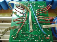
I don't know if you have read that in the past i had tried to lift this power gnd and leave the gnd for the two input filter capacitors (C14,C16) connected with a separate link to star gnd.
This configuration wasn't good.
See picture
Shaan thanks for the explain.
I don't know if you have read that in the past i had tried to lift this power gnd and leave the gnd for the two input filter capacitors (C14,C16) connected with a separate link to star gnd.
This configuration wasn't good.
See picture
Attachments
Last edited:
Thank you for the detailed explanation Shaan. I am wondering what the best way to mod this existing board so that the folks who recently got the GB boards can still have a functional amp without the noise and ground loop issues. The large caps are result of me optimizing for a robust square wave performance on simulation. It reduced the DC plateau sag on lower frequency square waves. So yes, probably excessive and maybe 470uF or 1000uF would have been fine. As far as the layout goes - that's not my expertise so I leave it up to guys like Marc and Sonal who were kind enough to provide their layouts. Despite all this, this amp sounds very very good and is one of my favorites. As I used a cap multiplier, I did not notice the hum issue. I imagine that if I fixed the ground issue and used the cap multiplier nownit will sound even better.
My thanks goes out to Thimios for being the pathfinder on this amp and for all the smart guys who helped Thimios to debug. It's a good conclusion and I am glad the riddle of the ground loop Sphinx was solved.
My thanks goes out to Thimios for being the pathfinder on this amp and for all the smart guys who helped Thimios to debug. It's a good conclusion and I am glad the riddle of the ground loop Sphinx was solved.
Last edited:
- Home
- Amplifiers
- Solid State
- CFH7 Amp