I hope the following is not interpreted as impolite...
Wow.
Yeah, I think I'd be switching to decaf in the very least.
OK. My point regarding debate has been missed: I'm not here (at least not in this particular thread) to cheer on and promote the cascode any more than I am my definite faith in God. I'd love to enter into "the cascode challenge", but that eventual thread will start with something like, "Hey audio fanatics, I love the cascode topology! Does anyone have any comments and technical support regarding its merits or pitfalls? I'd like to see what the rest of the world thinks about this fantastic circuit implementation!" But this thread did not. While there, I'd be prepared with interest in wondering why you don't use cascodes 90% of the time, here I am not, with my apology for this renewed attempt at being so direct.
I am not trying to be a cascode "evangelist"; It works very well for me when I use it (because I do so with careful discipline) and that is sufficient to satisfy me. Any address I have made to the merits of the cascode has been "unbiased" in the sense of statements like "using cascode to maintain collector voltage". That's like "using the gas pedal to open the throttle body butterfly". It would not mean I thought my car was faster than yours.
Rather, I was presenting a series of technical questions within the scope of using the cascode, i.e., if you generally don't prefer to implement the cascode, you would probably have little to offer, and that's perfectly acceptable.
The likely non-posting majority reading this post should agree based on the intro post, and their being here would surely be simply to see how my questions were answered, in case they face similar curiosity.
Generally, I'm wondering about possibilities for optimization of the cascode in cases where it MAY be indicated for usage. I now have some good answers to that end, but there are still a few unanswered points from my last post (or the one before that I guess), regarding minimizing the "evils" such as oscillation that might present with use of my proposed circuit (which I have already gladly conceded is not a new invention). At this point, I'm pretty much ready to conclude that my questions have been well-answered, with one exception. I'm still curious about responses to my speculation about what transistor parameters might be of highest priority in order to attain a successful implementation with what I'm calling a "cascode driven by a buffered signal-following reference..." Thank you to those who continue to offer your vast insights to me!!
Happy listening in the meantime, and ALL IN GOOD FUN!!
posted by lineup
... ... ... ...
Wow.
...COFFEE...
Yeah, I think I'd be switching to decaf in the very least.
OK. My point regarding debate has been missed: I'm not here (at least not in this particular thread) to cheer on and promote the cascode any more than I am my definite faith in God. I'd love to enter into "the cascode challenge", but that eventual thread will start with something like, "Hey audio fanatics, I love the cascode topology! Does anyone have any comments and technical support regarding its merits or pitfalls? I'd like to see what the rest of the world thinks about this fantastic circuit implementation!" But this thread did not. While there, I'd be prepared with interest in wondering why you don't use cascodes 90% of the time, here I am not, with my apology for this renewed attempt at being so direct.
I am not trying to be a cascode "evangelist"; It works very well for me when I use it (because I do so with careful discipline) and that is sufficient to satisfy me. Any address I have made to the merits of the cascode has been "unbiased" in the sense of statements like "using cascode to maintain collector voltage". That's like "using the gas pedal to open the throttle body butterfly". It would not mean I thought my car was faster than yours.
Rather, I was presenting a series of technical questions within the scope of using the cascode, i.e., if you generally don't prefer to implement the cascode, you would probably have little to offer, and that's perfectly acceptable.
The likely non-posting majority reading this post should agree based on the intro post, and their being here would surely be simply to see how my questions were answered, in case they face similar curiosity.
Generally, I'm wondering about possibilities for optimization of the cascode in cases where it MAY be indicated for usage. I now have some good answers to that end, but there are still a few unanswered points from my last post (or the one before that I guess), regarding minimizing the "evils" such as oscillation that might present with use of my proposed circuit (which I have already gladly conceded is not a new invention). At this point, I'm pretty much ready to conclude that my questions have been well-answered, with one exception. I'm still curious about responses to my speculation about what transistor parameters might be of highest priority in order to attain a successful implementation with what I'm calling a "cascode driven by a buffered signal-following reference..." Thank you to those who continue to offer your vast insights to me!!
Happy listening in the meantime, and ALL IN GOOD FUN!!
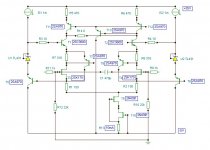
traderbam said:Here's that Halcro circuit in an easier to understand diagram.
They've used CFPs for the subtractor inputs to boost their gain, linearity and input impedance. They have then cascoded these with Q3 & Q4, referenced to the input emitters via V1. Then a second cascode with Q5 & Q6, this time referenced to the pos supply via V2. Q9 & Q10 form a current mirror that feeds the VAS amplifier, Q11, in turn cascoded by Q12. C1 is the miller cap.
Sorry I keep re-posting, but I almost forgot...
I still don't see the benefit of the "secondary" cascodes, referenced to positive rail. They are not in "common-base mode" with respect to the mirror components unless something is slipping past me here. All I can see is power supply ripple being unnecessarily injected into the "primary" cascode collectors, which would hopefully reject it, but their "lives" won't be made any easier in trying to establish a large PSRR, once again that's unless I'm missing something significant here. Semper curiosi. Thanks again for any insights.
acoustixman,
you can use cascodes in all stages. Tell us the purpose of that particular stage along with some other details, please.
you can use cascodes in all stages. Tell us the purpose of that particular stage along with some other details, please.
Me neither. I would certainly avoid them.I still don't see the benefit of the "secondary" cascodes, referenced to positive rail.
Lumba Ogir said:acoustixman,
you can use cascodes in all stages.
Agreed. I generally only use them for collector loads though.
Tell us the purpose of that particular stage along with some other details, please.
Kinda had to hammer this out quickly (at the office); please forgive my grammar
")
Frankly, what I had in mind is pretty similar to the diagrams you provided. I am currently using "signal ground" cascodes upon my diff amp tails (variously 15-30V rel to GND) and VAS legs (variously 3-5V rel to RAILS). The results to date have been quite excellent in the "standing up the hair on the back of the neck" category and I just want to see how deep this rabbit hole goes!
The essence of the plan I am investigating is to utilize the common mode signal (taken from between my emitter ballasts at current source node) as the cascode reference in the manner discussed herein. The diff amp Vce's should thus average to approximately constant (and BE constant with zero differential signal).
My rationale is that (1) I could reduce the cascode "voltage margin" and use higher hFE transistors in the diff amp [as I am currently using in the VAS - check out the Zetex ZTX688B and ZTX788B], simultaneously entertaining the use of quiet and temperature-stable zeners (rather than being in the noisy avalanche mode with the 15+V ones) and (2) achieve quicker transient response from the diff amp by further reducing Miller effect since there will be no "squeeze" from the relatively high impedance signal path; I expect that these aspects would be possible if the cascode were free to keep the Vce approximately constant [and small], RATHER than just keeping Vc-GND approximately constant [and large enough to give the illusion of keeping Vce approximately constant by reducing its proportionate change during common-mode excursions within the fixed cascode margin], knowing that the common mode signal may be upwards of a full volt from sources like CD players and "active" musical instruments.
--------------------
For example: If the common mode signal pushes a full volt, and I'm cascoded at 15+GND (lets say 14V effective), that reduces the MEDIAN margin to 13V, providing the Miller feedback path only slightly, and probably maintaining a good C:B gain regime, but using avalanche-mode reference diodes.
If the common mode signal pushes the same volt, and I'm cascoding at 5.6+GND (4.6V effective), the margin diminishes to 3.6V, I suppose the Miller load should be similar in either case but the transistor C:B gain parameters may be approaching some "knees" in the voltage-dependent curve. If I push that 5.6V up by the same full volt (assuming a convenient low-impedance source) instead, the 5V margin should go unaffected, correct? Now I don't even need to worry about the voltage-dependent gain curves. I'm using one point all the time. Plus I get to use nice [relatively quiet?] temperature-neutral 5.6V zener diodes (or nearby values as other junctions may indicate for minor temp coefficient compensation, maybe even green leds) for my references.
--------------------
I was thinking that the same thing could be done in the VAS in order to enable [larger voltage swing due to] higher ballast values to dissipatively increase linearity there as well without increasing the Miller effect "from below".
Another perspective: I guess in a very near sense I would be "BOOTSTRAPPING" the cascode drives (wasn't thinking of it that way at first since I'm not pushing anything past the rails like in an N-channel high-side PWM driver) so that when a gain transistor's emitter "draws up" to follow its base, its collector output voltage is simultaneously pushed up and the gain transistor never encounters a change in Vce.
Overall the project goal is a low OL gain, high dynamic range / "linear to the limits" amplifier. But then again, whose isn't?
acoustixman said:
Sorry I keep re-posting, but I almost forgot...
I still don't see the benefit of the "secondary" cascodes, referenced to positive rail. They are not in "common-base mode" with respect to the mirror components unless something is slipping past me here. All I can see is power supply ripple being unnecessarily injected into the "primary" cascode collectors, which would hopefully reject it, but their "lives" won't be made any easier in trying to establish a large PSRR, once again that's unless I'm missing something significant here. Semper curiosi. Thanks again for any insights.
Keep in mind that the whole Halcro amplifier works in inverting mode, which makes the cascodes even less useful here. PSRR still won't be great because of miller capacitor.
One great thing you can do with a cascode at input is to reference comp. capacitor to one of common base emitters. This gaves great PSRR, I tried it at one of my amps with success, the integrating loop around cascode/VAS needed its own compensation though.
Adam
Lumba Ogir said:acoustixman,
consider this circuit as a starting point.
Thanx a lot; I'll have to study more closely later though; busy day of coding at the orifice today!
darkfenriz said:...reference comp. capacitor to one of common base emitters...
By this, are you referring to the compensation capacitor also commonly known as the "dominant pole capacitor", popularly connected locally from output to [inverted] input of VAS, being connected instead from output of VAS to cascode node in diff amp (+inp) leg ("above" gain collector and "below" cascode emitter)? I can't presently visualize how this improves PSRR (or what else you might have meant by "comp. capacitor").
I'm not disputing your statement but would you help with a diagram snippet at your convenience?
acoustixman said:By this, are you referring to the compensation capacitor also commonly known as the "dominant pole capacitor", popularly connected locally from output to [inverted] input of VAS, being connected instead from output of VAS to cascode node in diff amp (+inp) leg ("above" gain collector and "below" cascode emitter)? I can't presently visualize how this improves PSRR (or what else you might have meant by "comp. capacitor").
In the schematic of this post, the left side of C1 should be connected not to the base of Q11, but to the junction of the emitter of Q6 and the collector of Q3. The DC reference voltage for the bases of Q5 and Q6 should be a zener or TL431 or similar, referenced to ground and not the positive supply, with the bias resistor for the reference going from the positive terminal of the reference to the positive supply. Compensation of this local feedback loop can be done with a series RC between the base of Q11 and the positive supply.
The math behind this was developed in an article called "A General Relationship Between Amplifier Parameters And Its Application To PSRR Improvement" by Sackinger, Goette and Guggenbuhl. It used to be available online, but I can't find it now. If you email me, I can send it to you.
acoustixman said:
Sorry I keep re-posting, but I almost forgot...
I still don't see the benefit of the "secondary" cascodes, referenced to positive rail. They are not in "common-base mode" with respect to the mirror components unless something is slipping past me here. All I can see is power supply ripple being unnecessarily injected into the "primary" cascode collectors, which would hopefully reject it, but their "lives" won't be made any easier in trying to establish a large PSRR, once again that's unless I'm missing something significant here. Semper curiosi. Thanks again for any insights.
Good question. I think the Halcro idea is that the VAS and current mirror should be referenced to the pos supply. So Q5 & Q6 help isolate the bases of Q3 & Q4 from common mode voltage. Imagaine, if you will, that the subtractor has one psu reference and the mirror/VAS has a separate one. It does not matter too much that they are separate in voltage provided the current is kept independent.
Andy's reference to rewiring to improve PSRR of the VAS output will work but only at the sacrifice of stability of the VAS. In my experience, it is nearly impossible to make the circuit adequately stable in this configuration. It is easier to attack the problem by stabilizing the psu.
traderbam said:Andy's reference to rewiring to improve PSRR of the VAS output will work but only at the sacrifice of stability of the VAS.
Yes, it definitely increases the local loop gain of the VAS, so steps need to be taken to stabilize it. The impedance of the junction of the base of Q11 and the collectors of Q6 and Q9 becomes large, needing a shunt element to tame it. Good layout is important too, as the oscillation wants to be around 20-50 MHz.
Good day to all...
Just thinking Q10 already "virtually cascoded" via diode connection... Q9 only sees the high-impedance side of Q6 so still not cascode on Q9... Worth some more study on my part I guess...
Except that these cascode-protected transistors will be multiplying nice and quickly and that should assist this semi-local loop's phase margin, true?
Maybe keep a "small pF" cap in the customary position and just let it fade above 20 mega?
Now I'm feeling just a little smarter at least... I promise I won't let it go to my head.
On a previous post I described a common mode follower only for the cascode but your post shows something that may be much better for its following of differential AND common mode signals in terms of preventing Vce changes from being applied to the gain transistors (T3, T4 {CFB:T7, T8}). The buffered cascode references (from sources of T3, T4) section of this meet my thoughts to a TEE and definitely demonstrates that this plan has some merits. I wonder if those TL431 1mA bias sources are active? I was thinking that wouldn't hurt either, provided their high impedance is sufficiently offset by the quantity of available current in terms of quickly charging the Miller capacitances. Darlington connection have any potential maybe?
edit: Of course good wide-band capacitive bypassing of voltage reference will be key so maybe impedance not a problem if done sufficiently?
If correct, I observe that we are basically looking at a differential output across R140 here, (the T2, T12) half of which could be neglected if the VAS were so configured.
traderbam said:
Good question. I think the Halcro idea is that the VAS and current mirror should be referenced to the pos supply. So Q5 & Q6 help isolate the bases of Q3 & Q4 from common mode voltage. Imagaine, if you will, that the subtractor has one psu reference and the mirror/VAS has a separate one. It does not matter too much that they are separate in voltage provided the current is kept independent.
Just thinking Q10 already "virtually cascoded" via diode connection... Q9 only sees the high-impedance side of Q6 so still not cascode on Q9... Worth some more study on my part I guess...
Andy's reference to rewiring to improve PSRR of the VAS output will work but only at the sacrifice of stability of the VAS. In my experience, it is nearly impossible to make the circuit adequately stable in this configuration. It is easier to attack the problem by stabilizing the psu.
Except that these cascode-protected transistors will be multiplying nice and quickly and that should assist this semi-local loop's phase margin, true?
andy_c said:
Yes, it definitely increases the local loop gain of the VAS, so steps need to be taken to stabilize it. The impedance of the junction of the base of Q11 and the collectors of Q6 and Q9 becomes large, needing a shunt element to tame it. Good layout is important too, as the oscillation wants to be around 20-50 MHz.
Maybe keep a "small pF" cap in the customary position and just let it fade above 20 mega?
Lumba Ogir said:Brian,
In your drawing the CCS to the bases of Q3/Q4 and Q12 is missing. Of course, the VAS should be referenced to the pos supply, it looks OK with Q5 & Q6 removed. I still don`t understand their intended role, for me that configuration is unacceptable anyway.
Now I'm feeling just a little smarter at least... I promise I won't let it go to my head.
Lumba Ogir said:...starting point... (schematic)
On a previous post I described a common mode follower only for the cascode but your post shows something that may be much better for its following of differential AND common mode signals in terms of preventing Vce changes from being applied to the gain transistors (T3, T4 {CFB:T7, T8}). The buffered cascode references (from sources of T3, T4) section of this meet my thoughts to a TEE and definitely demonstrates that this plan has some merits. I wonder if those TL431 1mA bias sources are active? I was thinking that wouldn't hurt either, provided their high impedance is sufficiently offset by the quantity of available current in terms of quickly charging the Miller capacitances. Darlington connection have any potential maybe?
edit: Of course good wide-band capacitive bypassing of voltage reference will be key so maybe impedance not a problem if done sufficiently?
If correct, I observe that we are basically looking at a differential output across R140 here, (the T2, T12) half of which could be neglected if the VAS were so configured.
acoustixman,
In my view:
-this is a very linear stage (even under demanding dynamic conditions).
-I would not apply GNF to this stage.
-I would only use it in balanced output mode.
-both the CFP and the cascode are prone to cause oscillations, if other types used:
-especially T3/T4 and T1/T2 should be selected carefully.
-T3/T4 should have very high (implemented) maximum operating frequency.
-please study the (astonishing) properties of T1/T2 thoroughly (not all may immediately be apparent).
-the CFP provides precise control of all parameters, inclusively DC stability.
-R14 (its value not defined) sets the gain.
-TL431 configured for 2.5V works fine @0.5mA, otherwise up to 36Vref @1.5mA,
typical dynamic impedance 0.2Ohm up to 100MHz, noise level 50nV / sqHz with fast and smooth turn-on characteristics.
For bypassing I would use high quality film capacitors aiming high frequency range.
Have a good day, Sir.
Lumba Ogir said:Brian,
In your drawing the CCS to the bases of Q3/Q4 and Q12 is missing. Of course, the VAS should be referenced to the pos supply, it looks OK with Q5 & Q6 removed. I still don`t understand their intended role, for me that configuration is unacceptable anyway.
I don't understand what you mean. I used voltage sources in my diagram; why are current sources needed?
I agree that the benefit that Q5 & Q6 provide appears to be very small. Why do you consider this configuration to be "unacceptable"?
acoustixman said:Just thinking Q10 already "virtually cascoded" via diode connection... Q9 only sees the high-impedance side of Q6 so still not cascode on Q9... Worth some more study on my part I guess...
Q9 sees the impedance of Q6, Q11 and C1.
Lumba Ogir said:acoustixman,
In my view:
-this is a very linear stage (even under demanding dynamic conditions).
-I would not apply GNF to this stage.
-I would only use it in balanced output mode.
-both the CFP and the cascode are prone to cause oscillations, if other types used:
-especially T3/T4 and T1/T2 should be selected carefully.
-T3/T4 should have very high (implemented) maximum operating frequency.
-please study the (astonishing) properties of T1/T2 thoroughly (not all may immediately be apparent).
-the CFP provides precise control of all parameters, inclusively DC stability.
-R14 (its value not defined) sets the gain.
-TL431 configured for 2.5V works fine @0.5mA, otherwise up to 36Vref @1.5mA,
typical dynamic impedance 0.2Ohm up to 100MHz, noise level 50nV / sqHz with fast and smooth turn-on characteristics.
For bypassing I would use high quality film capacitors aiming high frequency range.
sorry, 100KHz is more correct.
Have a good day, Sir.
And likewise. I'd be interested in being pointed to examples of utilizing a differential error signal as from this stage to drive outputs. I'm accustomed to referencing output to ground; but would this require "+ side" AND "- side" drivers/stages down the chain? I guess another way to ask this is "Are the speaker outputs differential too?"
traderbam said:I agree that the benefit that Q5 & Q6 provide appears to be very small. Why do you consider this configuration to be "unacceptable"?
Q9 sees the impedance of Q6, Q11 and C1.
It seems to me that these questions may address the same issue. The only 'benefit' the primary cascodes (Q3, Q4) receive from the secondary (Q5, Q6) is of having rail ripple voltage applied through a low-impedance load upon their collectors.
On your latter statement of what impedance Q9 sees, I didn't mean to seem ignorant; I was only speaking relative to Q6's possibilities; if it were a PNP transistor, at least we'd have some cascode benefit applied to the mirror output, and it wouldn't be imposing ripple energy upon Q3. It just seems like 2 steps ahead and 1 step behind. Applying a cascode to a cascode seems silly enough, but doing so with the nearest available dirty reference after we just got done enhancing the lower cascode reference for the error amp transistors seems ludicrous. In my version of comprehension it looks like we're using the signal path to provide a low-impedance link between input signal and power supply rail. There's usually no reason to ensure ripple-free rails; why introduce one?
It appears that the only 'benefit' the current mirror 'sees' is redundancy, in addition to the forwarding of whatever 'benefit' the primary cascodes may derive from driving their output current through rail ripple. I'd submit that this circuit would be much more equipped for PSRR, and no less apt for its existing merits, without Q5 & Q6 at all. A PNP cascode on Q9 would eat up the voltage margin for VAS base drive. Inverted cascode (which I don't claim to fully understand) could be interesting. I'd expect feedback to provide a 'cascode-like' effect to the mirror output anyway; base drive voltage to Q11 will surely not vary too much. No change to VAS (perfect use of such a voltage reference in rail-referenced stage); mirror input side gets no upper cascode since already in low-impedance diode mode.
[edit:] In any mention of cascode application to Q9, I mean to imply that the VAS drive signal would be established on the appropriate side of such an inclusion (i.e. 'south' of Q6 if it were a PNP cascode).
Lumba Ogir: Is this what you're saying too, or are we yet seeing different angles to it?
May the EMF be with you!
acoustixman,
I would go for fully balanced topology.And likewise. I'd be interested in being pointed to examples of utilizing a differential error signal as from this stage to drive outputs. I'm accustomed to referencing output to ground; but would this require "+ side" AND "- side" drivers/stages down the chain? I guess another way to ask this is "Are the speaker outputs differential too?"
I cannot see how Q5/Q6 could be helpful here. Each component should clearly enhance the sound and/or the function instead of merely being deteriorating.Lumba Ogir: Is this what you're saying too, or are we yet seeing different angles to it?
Attachments
acoustixman said:On your latter statement of what impedance Q9 sees, I didn't mean to seem ignorant; I was only speaking relative to Q6's possibilities; if it were a PNP transistor, at least we'd have some cascode benefit applied to the mirror output, and it wouldn't be imposing ripple energy upon Q3. It just seems like 2 steps ahead and 1 step behind. Applying a cascode to a cascode seems silly enough, but doing so with the nearest available dirty reference after we just got done enhancing the lower cascode reference for the error amp transistors seems ludicrous. In my version of comprehension it looks like we're using the signal path to provide a low-impedance link between input signal and power supply rail. There's usually no reason to ensure ripple-free rails; why introduce one?
I see what you mean. I see a problem with using a pnp as a cascode because you'd end up with two collectors joined together. I think Q6 has to be npn to pass Q3's current. As I see it, Q5 & Q6 are shielding Q9 and Q10. The latter don't need cascoding for Vce reasons as you've said; one has a diode and the other is fixed by Q11. You refer to the psu as being "dirty"...but why should it be dirty if regulated very well, which I assume it must be to keep the VAS output clean.
It appears that the only 'benefit' the current mirror 'sees' is redundancy, in addition to the forwarding of whatever 'benefit' the primary cascodes may derive from driving their output current through rail ripple. I'd submit that this circuit would be much more equipped for PSRR, and no less apt for its existing merits, without Q5 & Q6 at all.
It is worth checking out the CMRR and PSRR impact of Q5 & Q6 in simulation. I think they will add a benefit. My only question is about whether the benefit will be significant. We don't have the full circuit/layout. Halcro obviously think so.
traderbam said:...You refer to the psu as being "dirty"...but why should it be dirty if regulated very well, which I assume it must be to keep the VAS output clean.
I'd say we fully agree with just one caveat of mere opinion... I prefer to remove the requirement for power supply regulation via design of the amplifier itself. I agreed when I heard it said once by an audio 'pundit' (G. Randy Slone if I recall) that a regulated power supply doesn't necessarily do better than an amplifier at providing PSRR in principle. It's like using an amplifier (per DC level/polarity?) to power an amplifier. Just in the sense that making the amplifier circuit more complicated in a way that calls for complication of the power supply seems superfluous. Not necessarily bad (and I'm certainly not trying to argue), just not the way I'd do it. I generally stick with the "heavy toroids to beer-can-sized caps" approach to power supplies, with good quiet differential stages (and bypassing of the bias sources for cascodes and current sources as applicable; fc ~ 0.1 Hz) handling ripple-rejection. The cascode becomes the regulator for the sensitive parts that care at all about regulation; that's why I wouldn't cascode a cascode relative to an alternate rail potential (V+, V- vs GND). With a bunch of passive components ensuring DC to ripple-sensitive parts, themselves numbering few, I'll definitely take the Pepsi challenge against a regulated supply amplifier.
That's what brought me to my initial question; the merits of cascoding on the basis of referencing the signal waveform (representing something like a ripple influence, however "congruent" to the signal itself). My conclusion has become: If Miller effects and associated impedances are accounted for and/or minimized in the bandwidth of interest, biasing cascodes relative to the signal waveform can be made practicable to the end of containing the gain transistors at INDEED constant Vce. This of course based on assuming it is approached in a way that does not load or affect the input signal source.
It is worth checking out the CMRR and PSRR impact of Q5 & Q6 in simulation. I think they will add a benefit. My only question is about whether the benefit will be significant. We don't have the full circuit/layout. Halcro obviously think so.
True that is. I'd also like to do/see a simulation of this at some point. Now, to get around to acquiring some user-friendly simulation software somewhere...
Happy Monday!
- Status
- This old topic is closed. If you want to reopen this topic, contact a moderator using the "Report Post" button.
- Home
- Amplifiers
- Solid State
- Cascode Buffers