NON-linear interpolation
Hi dusfor99
Thanks for your tip [post #1115]
Have a look at [post #151]. Is this similar to what you were suggesting? if not I am very interested.
Did you take increasing and decreasing sample values into account?
The DAC outputs will switch as follows:
increasing sample:
( DAC1 )
( DAC1 )+( DAC2 )
( DAC1 )+( DAC2 )+( DAC3 )
( DAC1 )+( DAC2 )+( DAC3 )+(DAC4)
Decreasing sample:
( DAC1 )+( DAC2 )+( DAC3 )+(DAC4)
( DAC2 )+( DAC3 )+(DAC4)
( DAC3 )+(DAC4)
(DAC4)
The spaces are added to indicate amplitude.
So for the decreasing sample value, DAC sequence / I/V resistor values need to be different in order to obtain a symmetrical wave shape. For linear interpolation this makes no difference.
Another approach is changing the tap settings, this will ensure the correct waveform but introduces a constantly varying virtual sample-rate that introduces other problems.
Any Vacation Plan ????
Hi John,
I believe is a winter now in europe if you want to go a suny place just bought ticket to Indonesia and send me your flight number I will personally take you anywhere you want in Indonesia, just remeber to bring your PCB with you ok.
just give me info to :
moeh.anton at mailcity.com
Hi John,
I believe is a winter now in europe if you want to go a suny place just bought ticket to Indonesia and send me your flight number I will personally take you anywhere you want in Indonesia, just remeber to bring your PCB with you ok.
just give me info to :
moeh.anton at mailcity.com
Inverting BCK for DAC 2...n
Hi frbrw,
Thanks for your reply [post #1121]
Yes I am sure about that. The DAC's 2...n receive a delayed signal from the shiftregisters right? The shiftregisters output the new value at the positive going edge of BCK. So DAC's 2...n would sample both DATA and WS (on the positive going edge of BCK) about the same time the shiftregister outputs change. This could still work due to small timing delays as it did in my early prototype, but it remains critical and I don't like that. after inverting BCK for DAC's 2...n, it worked rock-solid. Verification with the oscilloscope showed WS and DATA were now sampled correctly for DAC2...n..
Yes I am aware this causes a small timing difference (0.7us) between DAC1 and DAC2...n, but listening sessions showed, it was not audible. But if it needs correction, a addittional 1 BCK delay could be used for WS and DATA, so BCK for DAC1 could then be inverted as well, and all DAC chip's would run exactly synchronous again. I will have a look if I can make this small modification in the PLD.
-ecdesigns- said:
As for jitter sensitivity, the D-I DAC's are comparable to NOS DAC's as no oversampling is used.
Could you explain, why ?
You have timing intervals between DAC chips that are 1/8 of non os.
IMHO the effect could be attenuated because multiple DAC chips convert the same original sample at a point in time.
Also the original sample needs 8 clockcycles to change completely, so for one original sample the clock is averaged over 8 cycles ??? Looks like a more complex jitter ( spread jitter spectrum ) that could sound different than non os or standard os.
Your DAC is hardware oversampling.
Anyway, my own experience is that non os sounds better than os but I don't know if this is because of jitter or something else related to the os chip or the DAC chip.
Re: Inverting BCK for DAC 2...n
Can't say I see the issue with clocking on the rising edge. Surely, for synchronicity you want everything triggering off the same edge. The '164's are basically a series of flipflops in sequence and one can think of the input register of the dac as a continuation of that. If one looks at the provided timing diagrams for the '1543 and the '164 data is static at the rising edge if setup and hold tome is met and the transition area is centred around the falling edge of the clock.
-ecdesigns- said:Hi frbrw,
Thanks for your reply [post #1121]
Yes I am sure about that. The DAC's 2...n receive a delayed signal from the shiftregisters right? The shiftregisters output the new value at the positive going edge of BCK. So DAC's 2...n would sample both DATA and WS (on the positive going edge of BCK) about the same time the shiftregister outputs change. This could still work due to small timing delays as it did in my early prototype, but it remains critical and I don't like that. after inverting BCK for DAC's 2...n, it worked rock-solid. Verification with the oscilloscope showed WS and DATA were now sampled correctly for DAC2...n..
Can't say I see the issue with clocking on the rising edge. Surely, for synchronicity you want everything triggering off the same edge. The '164's are basically a series of flipflops in sequence and one can think of the input register of the dac as a continuation of that. If one looks at the provided timing diagrams for the '1543 and the '164 data is static at the rising edge if setup and hold tome is met and the transition area is centred around the falling edge of the clock.
Bernhard said:
Could you explain, why ?
None of the individual dacs run faster than Fs.
You have timing intervals between DAC chips that are 1/8 of non os.
IMHO the effect could be attenuated because multiple DAC chips convert the same original sample at a point in time.
Also the original sample needs 8 clockcycles to change completely, so for one original sample the clock is averaged over 8 cycles ??? Looks like a more complex jitter ( spread jitter spectrum ) that could sound different than non os or standard os.
Your DAC is hardware oversampling.
Anyway, my own experience is that non os sounds better than os but I don't know if this is because of jitter or something else related to the os chip or the DAC chip.
Oversampling takes a weighted average of a number of samples and sums them to create a new sample. You can do this in the analogue or digital domain. The linear in linear interpolation refers to the weighting of the samples i.e. they are linearly weighted. Each new sample is made up of a linearly weighted average of the current and previous sample. The main point here is that the summing is done in the analogue domain. The original samples only exist in the digital domain and the new combined sample only exists in the analogue domain. Like all engineering it is a trade off. Many slower dacs for one fast one.
D-I 16 / octal D-I DAC comparison
Hi Rembulan,
Thanks for your kind invitation [post #1123] and your compliments [post#1084]
As you mention holliday's, this is the 16th year in a row without a holliday for me. yes believe it or not but I have been working almost continuously for 16 years now.
I also feel responsible to get the DAC kits ready as soon as possible like I promised, so a holliday is out of the question right now. I know some diyAudio members have already bought DAC chip's for this project and I don't like keeping them waiting longer than necessary.
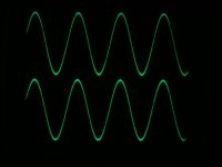
But now something different, I tested the new D-I 16 core this weekend, comparing it with the octal D-I DAC. I even added a oscillogram comparing the D-I 16 output (upper trace) with the octal D-I DAC core (lower trace), I had to use a 7 KHz sinewave and adjust lighting conditions to make the interpolated steps visible, of the octal D-I DAC core that is, the D-I 16 output is so smooth, no steps show up here. Needless to say both output signals are unfiltered, straight out of the diff amp.
As already noted, performance of the D-I 16 core comes very close to the octal D-I DAC, with a lot of music tracks there isn't even a difference audible. One has to listen very carefully to hear the subtle differences, first of all the D-I 16 core has a slightly warmer midrange and a smoother sound. However, the low distortion of the octal D-I DAC based on the TDA1541A starts showing as one focusses on the sound detail. But when compared to the much more complex design of octal D-I DAC core with relatively expensive DAC chips, the D-I 16 core is amazing.
Hi Rembulan,
Thanks for your kind invitation [post #1123] and your compliments [post#1084]
As you mention holliday's, this is the 16th year in a row without a holliday for me. yes believe it or not but I have been working almost continuously for 16 years now.
I also feel responsible to get the DAC kits ready as soon as possible like I promised, so a holliday is out of the question right now. I know some diyAudio members have already bought DAC chip's for this project and I don't like keeping them waiting longer than necessary.
But now something different, I tested the new D-I 16 core this weekend, comparing it with the octal D-I DAC. I even added a oscillogram comparing the D-I 16 output (upper trace) with the octal D-I DAC core (lower trace), I had to use a 7 KHz sinewave and adjust lighting conditions to make the interpolated steps visible, of the octal D-I DAC core that is, the D-I 16 output is so smooth, no steps show up here. Needless to say both output signals are unfiltered, straight out of the diff amp.
As already noted, performance of the D-I 16 core comes very close to the octal D-I DAC, with a lot of music tracks there isn't even a difference audible. One has to listen very carefully to hear the subtle differences, first of all the D-I 16 core has a slightly warmer midrange and a smoother sound. However, the low distortion of the octal D-I DAC based on the TDA1541A starts showing as one focusses on the sound detail. But when compared to the much more complex design of octal D-I DAC core with relatively expensive DAC chips, the D-I 16 core is amazing.
Attachments
rfbrw said:
None of the individual dacs run faster than Fs.
Oversampling takes a weighted average of a number of samples and sums them to create a new sample. You can do this in the analogue or digital domain. The linear in linear interpolation refers to the weighting of the samples i.e. they are linearly weighted. Each new sample is made up of a linearly weighted average of the current and previous sample. The main point here is that the summing is done in the analogue domain. The original samples only exist in the digital domain and the new combined sample only exists in the analogue domain. Like all engineering it is a trade off. Many slower dacs for one fast one.
It is not important how fast one single DAC runs and if the new sample is created in the analog or digital domain.
Important is only how the waveform looks in the summing junction.
You are not listening to each of 8 DACs but to all of them together.
A non os DAC has a time span of 22µs +/- delta t_jitter for one analog level step.
The 8x DI has a time span of 2,8µs +/- delta t_jitter for one analog level step.
Same as with a standard 8x os filter.
Displace one sample of a non os DAC by 2,8µs and do the same for one sample of one DAC chip of the 8 DI DAC.
How does that look like ?
Your DAC is hardware oversampling.
Bernhard is right here,
Useing the 8X core from ecdesigns you get an output sample rate of 8*FS. If the values are all equaly weighted (which is what they are) it is the EXACT same thing as oversampling by 8 and puting it through a FIR filter with the coefficients of [1 1 1 1 1 1 1 1] This is "linear interpolation" Simply take the FFT of a rectangular box that is 1/FS wide (you will get a sinc function frequency responce and that is the "filter" you are creating in the analog domain. This is why I suggested to weight the ouputs of each DAC, that way you change the filter frequncy responce. Ideally since it is a NON OS DAC you should compensate for the SINC rolloff caused by the "upsampling" process tht is really going on here. But this is all the technical stuff, what we can really see matters is how someone percieves the sound that comes out the DAC.
Jitter.
By using 8 analog DAC's to create 1 output sample, the overall DAC has now have some "jitter rejection" Think of it this way. In the NOSDAC the output changes from S
") to S(n+1) at a rate of 1/FS. So if there was a jitter (delta T) on the clock edge that this change occured, then you would have a error in the output of (delta T*(S(n+1) - S)). When you have a DAC like ecdesigns (or any OS DAC for that matter) the error in the output is divided by the OS factor. So for the 8 DAC design, the error would be (delta T* S(n+1) - S)/8 since changing 1 DAC output can only move the output by 1/8th now. So now your going to say, haaa, I got you, there are actualy 8 of these errors in edesigns DAC in teh same time a NOS DAC only gets 1. But just wait, There are 2 things to note here.
to S(n+1) at a rate of 1/FS. So if there was a jitter (delta T) on the clock edge that this change occured, then you would have a error in the output of (delta T*(S(n+1) - S)). When you have a DAC like ecdesigns (or any OS DAC for that matter) the error in the output is divided by the OS factor. So for the 8 DAC design, the error would be (delta T* S(n+1) - S)/8 since changing 1 DAC output can only move the output by 1/8th now. So now your going to say, haaa, I got you, there are actualy 8 of these errors in edesigns DAC in teh same time a NOS DAC only gets 1. But just wait, There are 2 things to note here. 1. The jitter is now spread over time.
2. The jitter is not jsut added together to get a total jitter. I depends on the nature of the jitter. I would say (now this is a guess I admit) that the jitter has some statistical property to it, perhapsl like some gaussian shape. So you cannot say that 8 jitter errors at 1/8th the amplitude, would actually add up to 1 jitter error with a amplitude of 1.
Ecdesigns, your DAC is very cool. The most ompressive thing about it to me is the the shear magnitude of components that you have connected together and still get great sound. I would like to send you a DAC design of mine and get you to rates is qaulity as far as sound goes. I just design by the SPEC but honestly dont have the "golden ears" to see if it is "warm" "smooth" and all the other terms people talk about. Let me know if you are interested.
CLD
Bernhard said:Always the same story, rfbrw.
I know, it's my fault. I ought to know by now that there is little point in attempting to deploy reason where you are concerned.
Hi Ecdesigns,
The weighting I was talking about is not the same as in post 151. With the topology you have. (upsample by N with N DACS) you cannot make a "great" non-linear filter. You will be able to get back a couple dB's of loss at the high end your topology currently has, but thats aobut it. (Ive been messing with simulations trying to see what can be done). I do one way you can get a real good analog OSF (linear phase) but it would require significant changes to your design, so I dont think its in the scope of what your trying to accomplish.
CLD
progress report
Hi EC.
You guessed right I didn't not have BCK inverted on DAC2, 3 and 4. I missed this bit of information in the thread.
They are inverted now.
The sound is better, the jittery time smear is gone. I am starting to hear the potential now. I will add the other 4 DAC chips this week and try to improve the supply to the logic tower.
~~~~~~
off topic:
Today I also learned to not ground all the unused pins on inverting buffers the hard way
I can now remove and reattach the logic tower in 30 minutes.
Putting the DAC back into parallel mode takes 5 minutes once the logic tower is removed. The logic tower is now 17 SMD chips tall.
Cheers,
Brent
D-I 16 power supply completed / redesigns
Hi all,
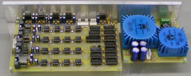
Project update, the D-I 16 core power supply is ready.
I added a photograph of both the D-I 16 core and the small power supply I designed for it. I used 2 separate encapsulated torroidial transformers to reduce power dissipation (low voltage for logic and TDA1543's and higher voltage for the OP-amps). Like the octal D-I DAC power supply, mains voltage selection is integrated (jumpers). The power supply PCB is single-sided. If desired, a relay can be mounted to provide remote ON/OFF function, if not, a wire jumper can be used instead like on the photograph. The rectifier diodes are fast BYV26E types (1KV). The power supply has a integrated mains filter.
In the background is one of the 8mm thick aluminum side panels of the new housings, it will also be used as heatsink. These side-panels will be used for all projects, the octal D-I DAC, the D-I 16 DAC, the control amplifier and the mosfet power amplifier monoblocks.
I am planning to modify the USB interface, I am going to integrate a automatic I2S switch, providing a external I2S input, and some logic to control the indicator LED and logo backlighting. The output is single-ended I2S, so it can be directly connected to the D-I 16 core. This module can also be used in the octal D-I DAC, greatly simplifying it's design. When using the USB interface as a separate module, it already outputs a single-ended I2S signal and provides a extra differential I2S input, in this case only a 5V supply has to be provided to power the I2S buffers and the logic. The USB input has the highest priority and overrules the differential I2S input.
Next on the agenda is redesigning the octal D-I DAC power supplies, making them more compact and simplify them where possible. I also need to redesign the tube output modules, placing the tube sockets on the component side and reduce PCB dimensions.
I am also considering using the mixed mode exclusively as this definately produces the best sound quality by far, this way the analog output attenuator module can be left out as well. Now the system controller can also be removed, again simplifying the design.
By these redesigns, the octal D-I DAC can be made less complicated, while still providing exactly the same sound quality as the prototype. If desired, the D-I 16 core can be placed in the large octal D-I DAC housing as well. Now the D-I 16 core can also have a mixed mode output.
Hi all,
Project update, the D-I 16 core power supply is ready.
I added a photograph of both the D-I 16 core and the small power supply I designed for it. I used 2 separate encapsulated torroidial transformers to reduce power dissipation (low voltage for logic and TDA1543's and higher voltage for the OP-amps). Like the octal D-I DAC power supply, mains voltage selection is integrated (jumpers). The power supply PCB is single-sided. If desired, a relay can be mounted to provide remote ON/OFF function, if not, a wire jumper can be used instead like on the photograph. The rectifier diodes are fast BYV26E types (1KV). The power supply has a integrated mains filter.
In the background is one of the 8mm thick aluminum side panels of the new housings, it will also be used as heatsink. These side-panels will be used for all projects, the octal D-I DAC, the D-I 16 DAC, the control amplifier and the mosfet power amplifier monoblocks.
I am planning to modify the USB interface, I am going to integrate a automatic I2S switch, providing a external I2S input, and some logic to control the indicator LED and logo backlighting. The output is single-ended I2S, so it can be directly connected to the D-I 16 core. This module can also be used in the octal D-I DAC, greatly simplifying it's design. When using the USB interface as a separate module, it already outputs a single-ended I2S signal and provides a extra differential I2S input, in this case only a 5V supply has to be provided to power the I2S buffers and the logic. The USB input has the highest priority and overrules the differential I2S input.
Next on the agenda is redesigning the octal D-I DAC power supplies, making them more compact and simplify them where possible. I also need to redesign the tube output modules, placing the tube sockets on the component side and reduce PCB dimensions.
I am also considering using the mixed mode exclusively as this definately produces the best sound quality by far, this way the analog output attenuator module can be left out as well. Now the system controller can also be removed, again simplifying the design.
By these redesigns, the octal D-I DAC can be made less complicated, while still providing exactly the same sound quality as the prototype. If desired, the D-I 16 core can be placed in the large octal D-I DAC housing as well. Now the D-I 16 core can also have a mixed mode output.
Attachments
Hi EC
I've been following this most interesting thread from the beginning and would like to take this opportunity to congratulate you on your brilliant work.
I noticed that you will include a relay on the power supply board and was wondering if this will be switched by the USB module to ensure no popping occurs when the computer system is powered on/off. I don't know if this will be an issue with your design, but I have noticed this feature included in a commercially available USB DAC.
New USB module PCB design ready
Hi alleycat,
Thanks for the compliments [post #1137]
The relay on the D-I 16 power supply can only be controlled by a external device like a control amplifier. If this setup is not used, the relay is not assembled and a wire bridge placed across the relay contact connections on the PCB to enable power. The D-I 16 DAC still has a mains switch of course. The USB voltage is only used to toggle beteen USB input and the extra differential I2S input automatically, the selected source is indicated by a multicolour LED on the front panel. When pulling the USB plug, or switching-off the computer, the octal D-I DAC / D-I 16 DAC doesn't produce a click or pop, with the new USB interface, it also immediately switches to the external DI2S input.
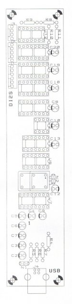
I finished the USB/DI2S/indicator module PCB design today. Now the automatic input switch and indicator LED control are also integrated. I added a silkscreen plot of this new module. So the complete D-I 16 DAC will basically consist of 3 modules:
- The D-I 16 power supply
- The D-I 16 core
- The USB/DI2S/indicator module
Using the same technique for the octal D-I DAC would limit the necessary modules to:
- The octal D-I DAC main power supply
- The octal D-I DAC core (11 small PCB's and one analog mainboard) or the single PCB D-I 16 core
- The USB/DI2S/indicator module
if the mixed mode output is also added:
- Tube diff. amplifier module (both channels will probably be placed on one PCB)
- Tube power supply
Hi alleycat,
Thanks for the compliments [post #1137]
The relay on the D-I 16 power supply can only be controlled by a external device like a control amplifier. If this setup is not used, the relay is not assembled and a wire bridge placed across the relay contact connections on the PCB to enable power. The D-I 16 DAC still has a mains switch of course. The USB voltage is only used to toggle beteen USB input and the extra differential I2S input automatically, the selected source is indicated by a multicolour LED on the front panel. When pulling the USB plug, or switching-off the computer, the octal D-I DAC / D-I 16 DAC doesn't produce a click or pop, with the new USB interface, it also immediately switches to the external DI2S input.
I finished the USB/DI2S/indicator module PCB design today. Now the automatic input switch and indicator LED control are also integrated. I added a silkscreen plot of this new module. So the complete D-I 16 DAC will basically consist of 3 modules:
- The D-I 16 power supply
- The D-I 16 core
- The USB/DI2S/indicator module
Using the same technique for the octal D-I DAC would limit the necessary modules to:
- The octal D-I DAC main power supply
- The octal D-I DAC core (11 small PCB's and one analog mainboard) or the single PCB D-I 16 core
- The USB/DI2S/indicator module
if the mixed mode output is also added:
- Tube diff. amplifier module (both channels will probably be placed on one PCB)
- Tube power supply
Attachments
Re: New USB module PCB design ready
Hi EC
Thanks for your reply.
An elegant solution. I should have known you'd be a step ahead of me!
Hi EC
Thanks for your reply.
-ecdesigns- said:The USB voltage is only used to toggle beteen USB input and the extra differential I2S input automatically, the selected source is indicated by a multicolour LED on the front panel. When pulling the USB plug, or switching-off the computer, the octal D-I DAC / D-I 16 DAC doesn't produce a click or pop, with the new USB interface, it also immediately switches to the external DI2S input.
An elegant solution. I should have known you'd be a step ahead of me!
Yes it fits
Hi all,
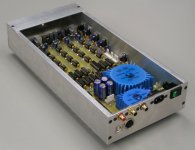
Today was a good day for designing and building housings, for the D-I 16 DAC that is. I added a photograph of the D-I 16 housing. As you can see I just managed to fit all modules, connectors and switches in. It's a very compact housing. The side panels are made of solid 8mm aluminum, the other panels are 2mm thick aluminum. The feet are 20mm diameter and 12 mm high, they are turned out of a tough black coloured plastic, acetal copolymer. They have adhesive rubber discs mounted to avoid scratches. The front panel is made of 2 aluminum profiles and a high-gloss stainless steel sheet.
At the rear, there are the RCA sockets for both right and left channel (red and white), and the RCA socket for remote power input (blue). Below the RCA sockets is the USB connection and the DI2S connection. Further to the right are the mains connection and mains switch. The RCA connectors are mounted on a transparent polycarbonate sheet for insulating them from the chassis.
The power supply PCB is mounted on top of a transparent polycarbonate sheet as well, preventing any contact of the PCB connections with the housing. All voltage regulators are mounted to a aluminum side panel, to ensure optimal cooling.
I still have to manufacture the new USB PCB that fits on the left side panel, and a small PCB for the LED indicator and logo backlighting, that has to be mounted behind the front panel.
Hi all,
Today was a good day for designing and building housings, for the D-I 16 DAC that is. I added a photograph of the D-I 16 housing. As you can see I just managed to fit all modules, connectors and switches in. It's a very compact housing. The side panels are made of solid 8mm aluminum, the other panels are 2mm thick aluminum. The feet are 20mm diameter and 12 mm high, they are turned out of a tough black coloured plastic, acetal copolymer. They have adhesive rubber discs mounted to avoid scratches. The front panel is made of 2 aluminum profiles and a high-gloss stainless steel sheet.
At the rear, there are the RCA sockets for both right and left channel (red and white), and the RCA socket for remote power input (blue). Below the RCA sockets is the USB connection and the DI2S connection. Further to the right are the mains connection and mains switch. The RCA connectors are mounted on a transparent polycarbonate sheet for insulating them from the chassis.
The power supply PCB is mounted on top of a transparent polycarbonate sheet as well, preventing any contact of the PCB connections with the housing. All voltage regulators are mounted to a aluminum side panel, to ensure optimal cooling.
I still have to manufacture the new USB PCB that fits on the left side panel, and a small PCB for the LED indicator and logo backlighting, that has to be mounted behind the front panel.
Attachments
- Home
- Source & Line
- Digital Line Level
- Building the ultimate NOS DAC using TDA1541A