PCM1704 forms two 23-bit segments from the input 24-bit code within itself.
Correct.
From the 16-bit code (in the format of OB or TWC), you can form two 15-bit segments.
Correct, but you needn´t input only 16 bits. With the logic circuit posted by John (ECDesigns), in conjunction with both channels of one TDA1541 chip, you can input 17 bits and you get all 2^17 = 131072 possible output values, making the arrangement a 17 bit dac.
There is simply no physical 17th bit in the digital domain i.e the dac. It is an equivalence that is a function the summed output current of the two dacs. You may have seen the relevant BB datasheets but it would seem you do not understand them. Or binary addition.
Rfbrw, see the post above. I cannot put it any simpler than that.
Thanks,
Alex
When you see that people spend their time on unrealizable illusions, it's a sin not to warn them about it. I think so. Do you think otherwise?Be careful what you wish for.
Hi Alex,
No, it's not. How do you not understand that the TDA1541 chip perceives the data in its input registers as a signed number (OB- or TWC-format). And the most significant bit is perceived as a sign. The TDA1541 chip can not work in another way, because it's so arranged. Using two channels of one TDA1541 chip or one channel from two TDA1541 chips, you will get two 15-bit Straight Binary segments.With the logic circuit posted by John (ECDesigns), in conjunction with both channels of one TDA1541 chip, you can input 17 bits...
When you see that people spend their time on unrealizable illusions, it's a sin not to warn them about it. I think so. Do you think otherwise?
Sometimes it maybe safer to leave them to their illusions. Failure might not necessarily push them into seeking greater understanding but instead push them into areas where a lack of understanding has serious consequences.
Oh bitty, bitty, bitty, bit. Wherever did that bitty go.
Alas, simply stating it does not make it so. Exactly where does the 17th bit go in a register that is only 16 bits long ? Show me the conversion of a 17bit word with either of the 16 bit dacs.
Rfbrw, see the post above. I cannot put it any simpler than that.
Thanks,
Alex
Alas, simply stating it does not make it so. Exactly where does the 17th bit go in a register that is only 16 bits long ? Show me the conversion of a 17bit word with either of the 16 bit dacs.
The TDA1541A is a great DAC, maybe the best ever. IMHO there are two things to take care if you want improve its performance.
Firstly I would avoid to get the MSB switching at every zero crossing, this causes glitch. Two's complement notation causes the MSB to switch at every zero crossing, while sign magnitude notation doesn't. So you should get the TDA working as a sign magnitude DAC, like the PCM1704.
To do the above you need the MSB does not switch at any time, since the TDA assumes it as the sign and so it will change its state at every zero crossing.
Finally, you loose 1 bit since the MSB does not swithc anymore, and then it remains 15 bit only to represent the signal.
Like the PCM1704 that uses 2 x 23 bit converter to get a 24 bit DAC, you have to use 2 x 15 bit converter to get a 16 bit DAC, so one TDA1541A per channel.
In this way you get a single TDA1541A that outputs 0 to -2mA from both channel where MSB never switchs. Then you have to combine both channel of a single TDA to get one channel to swing from +2mA to -2mA (16 bit again).
Secondly, but most important, I would take the maximum care of the timing of the TDA. The most important signal is the latch, not the bit clock.
So you should feed the WS input directly from a real low phase noise oscillator (2 osclillators if you want to play both sample rate families plus some programmable dividers if you need oversample).
The driver circuit should be slaved from the DAC: at every clock of the WS signal the driver circuit will provide 16 bits for each channel as faster as possible in simoultaneous mode (MSB fixed, never changes), then the bit clock will be stopped, to avoid any interference with the latch signal.
To do the job you need to implement a FIFO in the driver circuit because you have two different clock domains, the bit clock of the source and the Latch of the TDA1541A driven directly from the external low noise oscillator.
You can do the above with a FPGA.
Hi Alex,
No, it's not. How do you not understand that the TDA1541 chip perceives the data in its input registers as a signed number (OB- or TWC-format). And the most significant bit is perceived as a sign. The TDA1541 chip can not work in another way, because it's so arranged. Using two channels of one TDA1541 chip or one channel from two TDA1541 chips, you will get two 15-bit Straight Binary segments.
Serg, even though I have not built John´s circuit, I understand the chip well enough to tell you (and Rfbrw) that it will work and will result in a 17 bit dac.
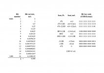
Inside the tda1541, each bit is associated with a value of current. All these currents have the same sign. They all flow in the same direction, altough they have different values.
The msb will switch a current of -2mA, that is all it does. The next bit is -1mA, the next -0.5mA, and so forth, down to the lsb which is -61nA aproximately.
Each channel has a range of current of -4mA (all bits on), to zero (all bits off). Since the summing of the currents of two channels occurs before any analog stage, the result of this sum can assume a value of -8mA to zero. It cannot assume a positive value.
In conclusion, it is not the chip that perceives the msb as a sign. It is your analog stage with a servo or coupling cap that does it, by removing the DC component. This is true for TDA1541.
Final note, we are summing the currents of two 16 bit dacs, where each can assume 65536 values. The result can assume 131072 values which corresponds to a resolution of 17 bits. This resolution can be realized with John´s circuit and with a 17 bit digital input.
Thanks,
Alex
Rfbrw, I did stick to the point on each and every post. Unlike you.
My only goal here is to explain the circuit as well as I can, so everybody understands.
The 17th bit is the original msb. It is sampled by the logic circuit. In a flip flop. It doesn´t need to go into either dac chip.
John explanation was through if you ask me.
Building the ultimate NOS DAC using TDA1541A
But not everybody understood, so we entered into a bit of an argument about it. Unpleasant if you ask me. But we kept going, trying to explain it. I´m sure many understood it perfecly, such as Shinja. I posted this to help grasp what the logic does.
Building the ultimate NOS DAC using TDA1541A
If you ask me, this is beaten to death at this point.
Hi AndreaThe TDA1541A is a great DAC, maybe the best ever. IMHO there are two things to take care if you want improve its performance.
Firstly I would avoid to get the MSB switching at every zero crossing, this causes glitch. Two's complement notation causes the MSB to switch at every zero crossing, while sign magnitude notation doesn't. So you should get the TDA working as a sign magnitude DAC, like the PCM1704.
To do the above you need the MSB does not switch at any time, since the TDA assumes it as the sign and so it will change its state at every zero crossing.
Finally, you loose 1 bit since the MSB does not swithc anymore, and then it remains 15 bit only to represent the signal.
Like the PCM1704 that uses 2 x 23 bit converter to get a 24 bit DAC, you have to use 2 x 15 bit converter to get a 16 bit DAC, so one TDA1541A per channel.
In this way you get a single TDA1541A that outputs 0 to -2mA from both channel where MSB never switchs. Then you have to combine both channel of a single TDA to get one channel to swing from +2mA to -2mA (16 bit again).
Secondly, but most important, I would take the maximum care of the timing of the TDA. The most important signal is the latch, not the bit clock.
So you should feed the WS input directly from a real low phase noise oscillator (2 osclillators if you want to play both sample rate families plus some programmable dividers if you need oversample).
The driver circuit should be slaved from the DAC: at every clock of the WS signal the driver circuit will provide 16 bits for each channel as faster as possible in simoultaneous mode (MSB fixed, never changes), then the bit clock will be stopped, to avoid any interference with the latch signal.
To do the job you need to implement a FIFO in the driver circuit because you have two different clock domains, the bit clock of the source and the Latch of the TDA1541A driven directly from the external low noise oscillator.
You can do the above with a FPGA.
thanks for infos... Cheers
Hi Alex,
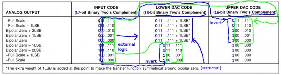
All is correct. But if you look at the coding scheme (COB-format), you can see that MSB has the value 1 for only one segment of values: from BPZ-LSB to -Full Scale (FS), and for another segment: from BPZ to + FS this value is 0, i.e. the MSB is actually a sign.The msb will switch a current of -2mA, that is all it does. The next bit is -1mA, the next -0.5mA, and so forth, down to the lsb which is -61nA aproximately.
You write it right, Alex. You do not take into account only one nuance: these 16 bits fall on the double amplitude of the signal (by two FS): from 0 to -4 mA. This range contains two 15-bits segments: from 0 to -2mA and from (-2mA+LSB) to -4mA. If you use two channels as a segmented DAC, then in each segment the current will change by 2mA: from 0 to -2mA ("lower DAC") and (from -2mA+LSB) to -4mA ("upper DAC"). And each segment will have 15 bits. As a result, it gives a 16-bit DAC.Each channel has a range of current of -4mA (all bits on), to zero (all bits off). Since the summing of the currents of two channels occurs before any analog stage, the result of this sum can assume a value of -8mA to zero. It cannot assume a positive value.
Attachments
17-bit signal from 16-bit format
If I understand correctly (please correct me if I am wrong), we do the conversion the following way:
There is an "upper" DAC e.g. the left channel within the TDA1541, and a "lower" DAC e.g. the right channel on the same chip. This way the symmetry of the positive and negative half cycle of the analog signal is provided.
The MSB of the original 16-bit signal gets stripped off. This bit will switch between the upper and lower DAC, it acts as a sign bit indeed.
But each DAC needs 16-bit input, how is it done? My interpretation is that each 15-bit stream is shifted 1-bit left. The leftmost bit will be the "new" MSB, and it will change from 0 to 1 at half-scale in each DAC (-6 dB analog level, where music instantaneous volume is loud). But now the LSB will be empty, 0. My idea is that it could be filled with a random bit, i.e. with dither. So we get 16-bit signal again in both the upper and lower DAC, and their combination is a true 17-bit DAC. We lose the sign bit, it won't enter in the DAC (its function will change) but since it is missing, we complete the 16-bit format at the LSB with a random bit. Essentially we get a 17-bit converter where the LSB is dither, and this converter has double digital range, resulting in double analog signal level.
That's it.The leftmost bit will be the "new" MSB, and it will change from 0 to 1 at half-scale in each DAC...
And what will it give? Why remove the MSB if: "The leftmost bit will be the "new" MSB"?My idea is that it could be filled with a random bit, i.e. with dither.
Serg, you are assuming a 16 bit digital input. That is where we differ.
If you only have 16 bits at the input then your segments are indeed 15 bits.
I am assuming a 17 bit digital input into the glue logic. The msb does not go into either dac, it just selects which dac receives the remaining 16 bits. We have two 16 bit segments.
The solution for outputting 17 good bits, with good dither, inside a 24 bit container, is done with a software player such as JRiver.
Thanks,
Alex
Code:
-FS         0 0000 0000 0000 0000    (dac#1 and dac#2 get all zeros)
-FS+1LSB    0 0000 0000 0000 0001    (dac#2 gets the data left shifted)

-0.5FS-1    0 0111 1111 1111 1111
-0.5FS      0 1000 0000 0000 0000

BPZ-1LSB    0 1111 1111 1111 1111    (dac#2 is "filled")
BPZ         1 0000 0000 0000 0000    (dac#2 gets all ones and dac#1 gets the data+1LSB)
BPZ+1LSB    1 0000 0000 0000 0001    (dac#1 gets 0000 0000 0000 0010)

+0.5FS      1 0111 1111 1111 1111    (dac#1 gets 1000 0000 0000 0000)
+0.5FS+1    1 1000 0000 0000 0000    (dac#1 gets 1000 0000 0000 0001)

+FS-1LSB    1 1111 1111 1111 1110    (dac#1 gets 1111 1111 1111 1111)
+FS         1 1111 1111 1111 1111    (can be avoided inside sofware player if needed)
Last edited:
Lcsaszar,
Your reasoning (for a 16 bits input) is correct, just a couple of details about the logic:
1 - The state of the msb also determines whether one dac receives all zeros or the other receives all ones.
2 - The state of the msb also determines if the data must receive addition of 1 LSB or not.
If your source is 16 bits, you can only form two 15 bit segments and you gain nothing by adding a random lsb. Better leave the lsb alone. (Just remember you need to add 1 LSB to one of the segments).
Good dither is a game changer, but must be done properly. You need higher than 17 bits source material and a good algorithm. This guy knows what he is doing: Not Just Another Dither/CD | Airwindows
(I´d ask him about making a 17 bit version, very easy for him, this would be minor changes in his source code.)
Thanks,
Alex
There is an "upper" DAC e.g. the left channel within the TDA1541, and a "lower" DAC e.g. the right channel on the same chip. This way the symmetry of the positive and negative half cycle of the analog signal is provided.
The MSB of the original 16-bit signal gets stripped off. This bit will switch between the upper and lower DAC, it acts as a sign bit indeed.
Your reasoning (for a 16 bits input) is correct, just a couple of details about the logic:
1 - The state of the msb also determines whether one dac receives all zeros or the other receives all ones.
2 - The state of the msb also determines if the data must receive addition of 1 LSB or not.
But each DAC needs 16-bit input, how is it done? My interpretation is that each 15-bit stream is shifted 1-bit left. The leftmost bit will be the "new" MSB, and it will change from 0 to 1 at half-scale in each DAC (-6 dB analog level, where music instantaneous volume is loud). But now the LSB will be empty, 0. My idea is that it could be filled with a random bit, i.e. with dither. So we get 16-bit signal again in both the upper and lower DAC, and their combination is a true 17-bit DAC. We lose the sign bit, it won't enter in the DAC (its function will change) but since it is missing, we complete the 16-bit format at the LSB with a random bit. Essentially we get a 17-bit converter where the LSB is dither, and this converter has double digital range, resulting in double analog signal level.
If your source is 16 bits, you can only form two 15 bit segments and you gain nothing by adding a random lsb. Better leave the lsb alone. (Just remember you need to add 1 LSB to one of the segments).
Good dither is a game changer, but must be done properly. You need higher than 17 bits source material and a good algorithm. This guy knows what he is doing: Not Just Another Dither/CD | Airwindows
(I´d ask him about making a 17 bit version, very easy for him, this would be minor changes in his source code.)
Thanks,
Alex
Last edited:
Hi Alex,
You can not "shove" anything into TDA1541 except for 16 bits. The reason is simple: it has a 16-bit input register. For one sampling period, only the contents of this 16-bit register TDA1541 can be perceived as data, and nothing more. The colleague rfbrw already wrote about this.Serg, you are assuming a 16 bit digital input. That is where we differ.
If you only have 16 bits at the input then your segments are indeed 15 bits.
- Home
- Source & Line
- Digital Line Level
- Building the ultimate NOS DAC using TDA1541A