The only difference between offset binary and 2's complement is an inverted the MSB (sign). As an example of 4-bit number:
Offset binary - Wikipedia
There is no need to over-think the idea behind it. It's like a difference between unsigned numbers (OB) and signed numbers (2's complement). The range is exactly the same and the only difference is a different meaning of MSB bit.
Code:
 OB   <====>   2's complement
1111                0111
....                ....
0000                1000
Offset binary - Wikipedia
There is no need to over-think the idea behind it. It's like a difference between unsigned numbers (OB) and signed numbers (2's complement). The range is exactly the same and the only difference is a different meaning of MSB bit.
Last edited:
It's like a difference between unsigned numbers (OB) and signed numbers (2's complement).
Both OB and TWC contain the sign of a number.
The range is exactly the same and the only difference is a different meaning of MSB bit.
That's right, but in both cases, this bit contains the sign of a number. For the mantissa, only 15 bits remain.
Both OB and TWC contain the sign of a number.
That's right, but in both cases, this bit contains the sign of a number. For the mantissa, only 15 bits remain.
I wouldn't call it a sign bit in case of the format itself. It can be taken as such, but that's not the idea behind it. There is a reason why OB is used in unipolar projects while 2's complement is used in bipolar ones. The reason is quite simple - OB doesn't account for truly bipolar signals because the idea is exactly the same as representing unsigned numbers in a binary format.
TDA1541A is an unipolar D/A converter and there is no sign bit whatsoever. It sinks the current according to the digital data from 0 mA (maximum code value, e.g. 1111) to -4 mA (minimum code value, e.g. 0000). There is no sign bit because sign bit defines crossing over bipolar zero and that is not the case with TDA1541A simply because it's unipolar and there is no zero crossing in the output according to its digital input.
Have a look at the following quote from the link I did post:
Offset binary is often used in digital signal processing (DSP). Most analog to digital (A/D) and digital to analog (D/A) chips are unipolar, which means that they cannot handle bipolar signals (signals with both positive and negative values). A simple solution to this is to bias the analog signals with a DC offset equal to half of the A/D and D/A converter's range. The resulting digital data then ends up being in offset binary format.
Last edited:
There is no sign bit because sign bit defines crossing over bipolar zero and that is not the case with TDA1541A simply because it's unipolar and there is no zero crossing in the output according to its digital input.
In the case of 1541, the sign specifies the direction of the number change from the offset point: up or down.
A sign is needed, otherwise there will be uncertainty:
Binary__________________Hex
1111 1111 1111 1111_____FFF
0111 1111 1111 1111_____7FF
Without MSB these two codes will match, although they correspond to different numbers.
Hi rfbrw,
Good to see you on this thread again")
Of course not. I simply combine both channels of one TDA1541A (outputs connected together) to obtain one mono DAC with different properties. I basically create a dual segment converter using L and R channels for each segment.
For clarity, I select simultaneous mode (Offset Binary) pin 27 connected to -5V and I use the full scale of each channel for generating a combined output signal with 8mA full scale current.
I need one TDA1541A for each channel, so I need two for stereo.
I use a decoder that sends different codes to each channel. This is quite easy as I can feed in L and R channel data simultaneously.
The goal is eliminating the 0111111111111111 to 1000000000000000 bit toggle at the output signal zero crossing.
At the zero crossing one channel receives 1111111111111111 while the other channel receives 0000000000000000 at the same time.
When combining both I get -4mA plus 0mA = -4mA at the zero crossing.
Depending on signal polarity I step one segment down or the other segment up. This way I avoid all bits flipping over at the zero crossing.
The full scale output current equals 1111111111111111 combined with 1111111111111111 = -8mA
The lowest output current equals 0000000000000000 combined with 0000000000000000 = 0mA.
The real MSB (16 or 24 bit input) is not sent to any of the converters, it only controls the codes each segment receives. This input MSB is stored in an external memory (flip-flop) and is used by the decoder.
The MSB is removed from the segment data by shifting the data one position to the left so the MSB is removed. This frees up the LSB to accept data for 17 bits.
With 16 bits input data, the LSB of each segment is not used (set to either 0 or 1 depending on the code sequence). With 24 bit input data, all 16 bits of each segment are used (filled with data) and the 24 bits are truncated at 17 bits.
The smallest current step equals approx. 61nA and when each converter has 16 bit real world accuracy I get 17 bit output.
The sign bit (input data) controls the codes each segment receives and it swaps the active segment depending on input data polarity.
Good to see you on this thread again
So you folks think you can turn a COB/BTC dac into a straight binary dac. Interesting.
Of course not. I simply combine both channels of one TDA1541A (outputs connected together) to obtain one mono DAC with different properties. I basically create a dual segment converter using L and R channels for each segment.
For clarity, I select simultaneous mode (Offset Binary) pin 27 connected to -5V and I use the full scale of each channel for generating a combined output signal with 8mA full scale current.
I need one TDA1541A for each channel, so I need two for stereo.
I use a decoder that sends different codes to each channel. This is quite easy as I can feed in L and R channel data simultaneously.
The goal is eliminating the 0111111111111111 to 1000000000000000 bit toggle at the output signal zero crossing.
At the zero crossing one channel receives 1111111111111111 while the other channel receives 0000000000000000 at the same time.
When combining both I get -4mA plus 0mA = -4mA at the zero crossing.
Depending on signal polarity I step one segment down or the other segment up. This way I avoid all bits flipping over at the zero crossing.
The full scale output current equals 1111111111111111 combined with 1111111111111111 = -8mA
The lowest output current equals 0000000000000000 combined with 0000000000000000 = 0mA.
The real MSB (16 or 24 bit input) is not sent to any of the converters, it only controls the codes each segment receives. This input MSB is stored in an external memory (flip-flop) and is used by the decoder.
The MSB is removed from the segment data by shifting the data one position to the left so the MSB is removed. This frees up the LSB to accept data for 17 bits.
With 16 bits input data, the LSB of each segment is not used (set to either 0 or 1 depending on the code sequence). With 24 bit input data, all 16 bits of each segment are used (filled with data) and the 24 bits are truncated at 17 bits.
The smallest current step equals approx. 61nA and when each converter has 16 bit real world accuracy I get 17 bit output.
The sign bit (input data) controls the codes each segment receives and it swaps the active segment depending on input data polarity.
Hi JOSI1,
You are correct, my fault.
There will be a one sample (64 bit) delay between both, L and R channel as I clock out R sample #2 together with L sample #1.
When WSI = 0, Right sample #1 should enter the delay line (left justified data).
By the time WSI = 1 the complete Right #1 sample has been clocked into the delay line, waiting to be clocked out simultaneously with the Left #1 sample that needs no delay and comes after Right #1 sample.
This also means that the window signal (for gating BCKO, DOL and ROR) has to move from the WSI 0 area to the WSI 1 area as we can only start clocking out data after we clocked the R channel into the delay line and this happens when WSI = 0.
So we have to swap the channels (DOR becomes DOL, DOR becomes DOL) as the delayed sample will now hold R channel data and the direct sample will now hold L channel data.
Next we have to move the window from WSI = 0 area to WSI = 1 area.
This can be done by creating an inverted WS signal NWSI using a 74LVC1G04 or 74HC04 inverter.
Pin 12 from U4 (RST) is disconnected from WSI and connected to the inverter output NWSI. This way the counter starts counting when WSI goes high.
Pin 2 from U11 is disconnected from WSI and connected to the inverter output NWSI. This way the window signal is enabled when WSI goes high.
LEO can be left connected to WSI or can be connected to the inverter output NWSI, both should work.
Simultaneous Protocol Converter
Hello John,
is it possible that the converter described in post #7078/7079 (timing diagram/schematic) creates a delay of 64 BCK cycles between right and left
channel measured at the output of TDA1541A. With TDA1541A connected to
I2S there is no delay.
Thanks
You are correct, my fault.
There will be a one sample (64 bit) delay between both, L and R channel as I clock out R sample #2 together with L sample #1.
When WSI = 0, Right sample #1 should enter the delay line (left justified data).
By the time WSI = 1 the complete Right #1 sample has been clocked into the delay line, waiting to be clocked out simultaneously with the Left #1 sample that needs no delay and comes after Right #1 sample.
This also means that the window signal (for gating BCKO, DOL and ROR) has to move from the WSI 0 area to the WSI 1 area as we can only start clocking out data after we clocked the R channel into the delay line and this happens when WSI = 0.
So we have to swap the channels (DOR becomes DOL, DOR becomes DOL) as the delayed sample will now hold R channel data and the direct sample will now hold L channel data.
Next we have to move the window from WSI = 0 area to WSI = 1 area.
This can be done by creating an inverted WS signal NWSI using a 74LVC1G04 or 74HC04 inverter.
Pin 12 from U4 (RST) is disconnected from WSI and connected to the inverter output NWSI. This way the counter starts counting when WSI goes high.
Pin 2 from U11 is disconnected from WSI and connected to the inverter output NWSI. This way the window signal is enabled when WSI goes high.
LEO can be left connected to WSI or can be connected to the inverter output NWSI, both should work.
John, thanks for the explanation.
I disabled JRiver dither and I can turn on and off this plugin (NotJustAnotherCD) and I definitely hear it. Put the plugin after any processing such as EQ.
Free download and more info:
Not Just Another Dither/CD | Airwindows
For what lies behind this unique dither see:
NaturalizeDither | Airwindows
We could ask this developer about implementing the 17 bits version, as well as 18 bits and 20 bits for use with AD1865 and AD1862
Thanks,
Alex
With high resolution material, the choice of dither before truncation makes a significant difference in sound. I am using a free VST plugin: NotJustAnotherDither (actually I am using the 16 bits version: NotJustAnotherCD) and my impression is that it´s better than my player´s dither.With 24 bit input data, all 16 bits of each segment are used (filled with data) and the 24 bits are truncated at 17 bits.
I disabled JRiver dither and I can turn on and off this plugin (NotJustAnotherCD) and I definitely hear it. Put the plugin after any processing such as EQ.
Free download and more info:
Not Just Another Dither/CD | Airwindows
For what lies behind this unique dither see:
NaturalizeDither | Airwindows
We could ask this developer about implementing the 17 bits version, as well as 18 bits and 20 bits for use with AD1865 and AD1862
Thanks,
Alex
Simultaneous Protocol Converter
Hello John,
since I already finished my converter board I wonder if this delay is only a minor flaw
or is a correction necessary anyway.
Delay=22.6us @f=44.1KHz with sonic speed 343m/sec causes a displacement of left and right speaker of less than 1cm.
Hello John,
since I already finished my converter board I wonder if this delay is only a minor flaw
or is a correction necessary anyway.
Delay=22.6us @f=44.1KHz with sonic speed 343m/sec causes a displacement of left and right speaker of less than 1cm.
Hi John,
It is important not only to fill a 16-bit segment. Another important thing is how these data are interpreted, how the contents of the input registers are interpreted. And TDA1541 does it this way: MSB is a sign, and the remaining bits are a number.
It's a mystery to me why you do not understand this.
Regards,
Serg
With 24 bit input data, all 16 bits of each segment are used (filled with data) and the 24 bits are truncated at 17 bits.
It is important not only to fill a 16-bit segment. Another important thing is how these data are interpreted, how the contents of the input registers are interpreted. And TDA1541 does it this way: MSB is a sign, and the remaining bits are a number.
It's a mystery to me why you do not understand this.
Regards,
Serg
Re post 6226.
As things stand I fail to see how any of this can work. The view from the perspective of the dac seems not to have been taken into account. The dac will still respond to the MSB of the recoded word as it always does. It will see it as a sign-bit. I cannot see how stripping off the original sign-bit helps. As far as I can see, keeping the original sign-bit is essential.
As things stand I fail to see how any of this can work. The view from the perspective of the dac seems not to have been taken into account. The dac will still respond to the MSB of the recoded word as it always does. It will see it as a sign-bit. I cannot see how stripping off the original sign-bit helps. As far as I can see, keeping the original sign-bit is essential.
Last edited:
The dac will still respond to the MSB of the recoded word as it always does. It will see it as a sign-bit.
Just so.
So, how you guys understand how the PCM1704 sign magnitude DAC work?
PCM1704 converts the input signal in the format of OB or TWC to USB format. In this case, two 23-bit segments are obtained from the input 24-bit signal inside the chip.
Guys, look at it this way. Suppose we have 17 bits of good data coming from the dir. The format is two´s complement. We convert it to offset binary by inverting the msb only.
Now, if the msb is zero then dac#1 gets all zeros and dac#2 gets the data left shifted.
If the msb is one then dac#2 gets all ones and dac#1 gets the data left shifted plus one.
Thanks,
Alex
Now, if the msb is zero then dac#1 gets all zeros and dac#2 gets the data left shifted.
If the msb is one then dac#2 gets all ones and dac#1 gets the data left shifted plus one.
Code:
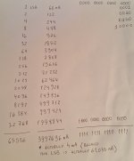
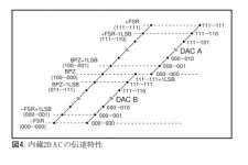
-FS         0 0000 0000 0000 0000    (dac#1 and dac#2 get all zeros)
-FS+1LSB    0 0000 0000 0000 0001    (dac#2 gets the data left shifted)

BPZ-1LSB    0 1111 1111 1111 1111    (dac#2 is "filled")
BPZ         1 0000 0000 0000 0000    (dac#2 gets all ones and dac#1 gets the data+1LSB)
BPZ+1LSB    1 0000 0000 0000 0001    (dac#1 gets 0000 0000 0000 0010)

+FS-1LSB    1 1111 1111 1111 1110    (dac#1 gets 1111 1111 1111 1111)
+FS         1 1111 1111 1111 1111    (hmmm....)
Thanks,
Alex
- Home
- Source & Line
- Digital Line Level
- Building the ultimate NOS DAC using TDA1541A