Hi studiostevus,
DEM clock frequency does not need to be equal to or a multiple of WS nor BCK. The DEM system can be viewed as a separate module that simply provides binary weighted DC bit currents for each channel.
The reasons I abandoned DEM oscillator synchronization are increased on-chip interference levels and the extra clock load on the super critical clock signals.
Two factors are most important:
1) DEM switch settling time.
2) Effectivity of active divider decoupling.
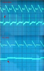
At higher DEM clock frequencies DEM switch settling time starts to get more impact on the averaged bit currents. Attached oscillograms illustrate this. Upper channel shows DEM oscillator output, lower channel shows unfiltered active divider output. Arrows show spike as a result of DEM switch settling time.
So here lower DEM clock frequency is clearly better.
At lower DEM clock frequencies however, RC filter efficiency reduces. The ripple currents that are visible on the lower channels need to be filtered out by the active divider decoupling caps. The higher the DEM clock frequency, the more effective the decoupling cap will be (lower ripple current) up to the point where series inductance will reduce decoupling efficiency.
So lowest DEM clock frequency is set by practical active divider decoupling cap value / size.
In practice we need to make a compromise between DEM clock frequency, impact of DEM switch settling time and ripple current on the active divider decoupling cap.
And with 1uF SMD 1210 size film decoupling caps this happens to be around 60 KHz.
John, fDEM of 60KHz? What brought along this odd frequency? Not a multiple of either ws or bck….
DEM clock frequency does not need to be equal to or a multiple of WS nor BCK. The DEM system can be viewed as a separate module that simply provides binary weighted DC bit currents for each channel.
The reasons I abandoned DEM oscillator synchronization are increased on-chip interference levels and the extra clock load on the super critical clock signals.
Two factors are most important:
1) DEM switch settling time.
2) Effectivity of active divider decoupling.
At higher DEM clock frequencies DEM switch settling time starts to get more impact on the averaged bit currents. Attached oscillograms illustrate this. Upper channel shows DEM oscillator output, lower channel shows unfiltered active divider output. Arrows show spike as a result of DEM switch settling time.
So here lower DEM clock frequency is clearly better.
At lower DEM clock frequencies however, RC filter efficiency reduces. The ripple currents that are visible on the lower channels need to be filtered out by the active divider decoupling caps. The higher the DEM clock frequency, the more effective the decoupling cap will be (lower ripple current) up to the point where series inductance will reduce decoupling efficiency.
So lowest DEM clock frequency is set by practical active divider decoupling cap value / size.
In practice we need to make a compromise between DEM clock frequency, impact of DEM switch settling time and ripple current on the active divider decoupling cap.
And with 1uF SMD 1210 size film decoupling caps this happens to be around 60 KHz.
Attachments
Hi Sandor
Highest average voltage on active divider outputs (pin 13 and pin 18) equals approx. -7.5V. Voltage on all other active divider outputs is lower. So 16V is safe.
I tested both, PPS (Panasonic) and FCA (Cornell Dubilier).
PPS: 16V, -40 to +85 Celcius, Dissipation factor 1.5%, IR > 300M Ohm (Panasonic Datasheet).
http://www.farnell.com/datasheets/31740.pdf
FCA: 16V, -40 to +85 Celcius, Dissipation factor, 1.5%, IR >300M Ohm (Cornell Dubilier datasheet).
http://www.farnell.com/datasheets/199119.pdf
In practice both work equally well.
They all are 16V, is this safe?
Highest average voltage on active divider outputs (pin 13 and pin 18) equals approx. -7.5V. Voltage on all other active divider outputs is lower. So 16V is safe.
Better a PPS (polyphenylene sulphide) or FCA (acrylic) dieletrcic?
I tested both, PPS (Panasonic) and FCA (Cornell Dubilier).
PPS: 16V, -40 to +85 Celcius, Dissipation factor 1.5%, IR > 300M Ohm (Panasonic Datasheet).
http://www.farnell.com/datasheets/31740.pdf
FCA: 16V, -40 to +85 Celcius, Dissipation factor, 1.5%, IR >300M Ohm (Cornell Dubilier datasheet).
http://www.farnell.com/datasheets/199119.pdf
In practice both work equally well.
Hi John,
thank you for answering.
1) I see that the Cornell-Dubilier datasheet explicitly states that their FCA acrylic film caps are "non-inductive". Could this be a REAL advantage (i.e. not only on paper) over Panasonic capacitors?
2) About the DEM clock frequency: have your ears confirmed the results shown by your scope, at 60 KHz?
3) As far as I understand, each of the decoupling caps should have its own route to pin 5. Is it acceptable to have a small "ground bus" in the center of the TDA1541, routed to pin 5 on one end?
Last edited:
poobah pointed out the problem of "direct interpolation" at #85 and so on.
Thank you, colleague Shinja
I am a sign with this post. But at these
early reports was not a refusal of initial concept.
Last edited:
Hi Sandor,
Both capacitors have stacked film construction (low inductance) and are very well suited for decoupling.
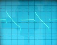
Yes, but I have to add that these tests were carried out with a modified free-running DEM oscillator circuit that offers very low jitter compared to the Philips datasheet application (attached oscillograms).
Yes, I also use a GND bus because of limited space for separate GND traces underneath the chip.
1) I see that the Cornell-Dubilier datasheet explicitly states that their FCA acrylic film caps are "non-inductive". Could this be a REAL advantage (i.e. not only on paper) over Panasonic capacitors?
Both capacitors have stacked film construction (low inductance) and are very well suited for decoupling.
2) About the DEM clock frequency: have your ears confirmed the results shown by your scope, at 60 KHz?
Yes, but I have to add that these tests were carried out with a modified free-running DEM oscillator circuit that offers very low jitter compared to the Philips datasheet application (attached oscillograms).
3) As far as I understand, each of the decoupling caps should have its own route to pin 5. Is it acceptable to have a small "ground bus" in the center of the TDA1541, routed to pin 5 on one end?
Yes, I also use a GND bus because of limited space for separate GND traces underneath the chip.
Attachments
Hi studiostevus,
DEM clock frequency does not need to be equal to or a multiple of WS nor BCK. The DEM system can be viewed as a separate module that simply provides binary weighted DC bit currents for each channel.
Although I am by no means an expert, I would think that although the DEM system can be viewed as a separate module (as can be seen indeed in the tda1541a internal schematic), spikes would nevertheless find their way to the substrate.
I realize this reasoning is has been argued by yourself some months ago, and I fully agree with ealier commenter's views on trial-and-error (which led to Edison's bulb), and that it is proper science to test a hypothesis and being honest if the hypothesis proves to be false.
Nevertheless, I would still be interested to understand the current views vs. earlier assumptions related to substrate bounce etc...
why?The reasons I abandoned DEM oscillator synchronization are increased on-chip interference levels
and the extra clock load on the super critical clock signals.
Hi maxlorenz,
In than is concluded your contribution? What you suggested? The number of the post?
You are not an attorney. The question was addressed an author of the subject. He capable answer the questions itself. And you are not a moderator, not you to solve that possible to write, but that no.
My contribution to development given project is an indication on inexactnesses and errors of the author of the subject.Again, SSerg, I fail to see how your posts contribute to anything at all...in the Universe.
In than is concluded your contribution? What you suggested? The number of the post?
This is not a forum for dialectic confrontation but for inventing, sharing and building nice gear to enjoy our beloved music. People who contribute freely to our enjoyment must be thanked and encouraged...
You are not an attorney. The question was addressed an author of the subject. He capable answer the questions itself. And you are not a moderator, not you to solve that possible to write, but that no.
Hi oshifis,
I used the call, which was kept at author message: «please feel free to ask, your comments, tips and reactions are very welcome» (post #1).And don't forget the principles described in the initial post
I call this a negative attitude. A more positive attitude would be something like this:
"Look, I don't like your solution for this and this reason. It can be done better. Here is the circuit diagram, photograph, and some measurements from the prototype of my solution - which I can demonstrate is better than your approach"
"Look, I don't like your solution for this and this reason. It can be done better. Here is the circuit diagram, photograph, and some measurements from the prototype of my solution - which I can demonstrate is better than your approach"
I must admit that I'm quite a bit puzzled by the idea of reducing the "DEM clock" freq down to 60Hz, with no other sinc pulse/clock involvement, but it's simple enough to try out and see what happens with my "much abused" old player .....
This dac chip continues to amaze, and I'm really pleased with the sound of Patrick's CEN o/p stage.
This dac chip continues to amaze, and I'm really pleased with the sound of Patrick's CEN o/p stage.
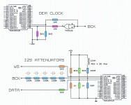
Hi tessier,
DATA and WS attenuators are designed for 3V3 signals (SD8-transport also outputs 3V3 signals).
For WS and DATA:
1K series resistor between digital audio source and TDA1541A I2S input.
680 Ohm pull-down resistor between TDA1541A I2S input and GND.
1K pull up resistor between TDA1541A I2S input and 3V3 (use digital audio source power supply).
Your I2S attenuators are designed for 5V TTL levels.
DATA and WS attenuators are designed for 3V3 signals (SD8-transport also outputs 3V3 signals).
Can you tell me the value of your I2S attenuators resistors for a 3.3V I2S ?
For WS and DATA:
1K series resistor between digital audio source and TDA1541A I2S input.
680 Ohm pull-down resistor between TDA1541A I2S input and GND.
1K pull up resistor between TDA1541A I2S input and 3V3 (use digital audio source power supply).
Hi studiostevus,
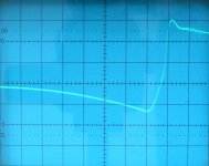
On-chip crosstalk cannot be avoided, but it can be lowered by reducing DEM oscillator frequency. Synchronising or triggering the DEM oscillator is possible (44.1 KHz with 2uF decoupling caps or 88.2 KHz with 1uF decoupling caps) but extra interference would be injected into the chip causing more problems. It is also essential that the free running DEM oscillator has low jitter, this cannot be guaranteed by the data sheet application (DEM timing cap pins 16 & 17 pick-up noise that then translates to jitter).
In order to get highest performance with the TDA1541A it is essential to minimise on-chip jitter by tuning external circuits.
I already applied I2S attenuators in earlier designs. I2S attenuators reduce signal amplitude, this reduces on-chip ground-bounce and related on-chip jitter.
Ground-bounce can also be lowered by reducing frequency. What's new is I2S signal band limiting that reduces the maximum fundamental frequency entering the DAC chip to approx. 2.8224 MHz.
Other cause for on-chip jitter is trigger uncertainty. Trigger uncertainty can be reduced by using cleanest possible supply voltages for both, -5V and +5V.
+5V supply ripple can be reduced to absolute minimum value by routing all bit currents back to +5V. Failing to do so will result in ripple on the +5V that relates to music content, causing on-chip deterministic jitter.
I/V circuits that result in relatively high on-chip deterministic jitter are:
- Low value I/V resistor between DAC output and GND.
- Diamond buffers.
- Op-amps.
These route selected bit currents to GND while unselected bit currents are internally routed to +5V.
Although I am by no means an expert, I would think that although the DEM system can be viewed as a separate module (as can be seen indeed in the tda1541a internal schematic), spikes would nevertheless find their way to the substrate.
On-chip crosstalk cannot be avoided, but it can be lowered by reducing DEM oscillator frequency. Synchronising or triggering the DEM oscillator is possible (44.1 KHz with 2uF decoupling caps or 88.2 KHz with 1uF decoupling caps) but extra interference would be injected into the chip causing more problems. It is also essential that the free running DEM oscillator has low jitter, this cannot be guaranteed by the data sheet application (DEM timing cap pins 16 & 17 pick-up noise that then translates to jitter).
In order to get highest performance with the TDA1541A it is essential to minimise on-chip jitter by tuning external circuits.
Nevertheless, I would still be interested to understand the current views vs. earlier assumptions related to substrate bounce etc…
I already applied I2S attenuators in earlier designs. I2S attenuators reduce signal amplitude, this reduces on-chip ground-bounce and related on-chip jitter.
Ground-bounce can also be lowered by reducing frequency. What's new is I2S signal band limiting that reduces the maximum fundamental frequency entering the DAC chip to approx. 2.8224 MHz.
Other cause for on-chip jitter is trigger uncertainty. Trigger uncertainty can be reduced by using cleanest possible supply voltages for both, -5V and +5V.
+5V supply ripple can be reduced to absolute minimum value by routing all bit currents back to +5V. Failing to do so will result in ripple on the +5V that relates to music content, causing on-chip deterministic jitter.
I/V circuits that result in relatively high on-chip deterministic jitter are:
- Low value I/V resistor between DAC output and GND.
- Diamond buffers.
- Op-amps.
These route selected bit currents to GND while unselected bit currents are internally routed to +5V.
Hello John,
Can I reduce this problem by disconnecting pins16/17 from the PCB and solder the timing cap (e.g. 1nF NPO 0603) directly to the IC pins 16/17.
Hi studiostevus,
It is also essential that the free running DEM oscillator has low jitter, this cannot be guaranteed by the data sheet application (DEM timing cap pins 16 & 17 pick-up noise that then translates to jitter).
.
Can I reduce this problem by disconnecting pins16/17 from the PCB and solder the timing cap (e.g. 1nF NPO 0603) directly to the IC pins 16/17.
Hi Jameshillj,
It's 60 KHz with 1uF decoupling caps. Typical DEM clock is 150KHz ... 250KHz with 100nF decoupling caps. By increasing decoupling cap value I can lower the DEM frequency while maintaining low ripple on the active divider outputs.
Today I tested 22KHz DEM frequency in combination with 2uF SMD film decoupling caps, (two stacked 1210 size caps on their side just fit underneath the TDA1541A and provide 1206 footprint). Seems lower DEM frequency is better, provided decoupling caps have large enough value for effective ripple attenuation.
I must admit that I'm quite a bit puzzled by the idea of reducing the "DEM clock" freq down to 60Hz
It's 60 KHz with 1uF decoupling caps. Typical DEM clock is 150KHz ... 250KHz with 100nF decoupling caps. By increasing decoupling cap value I can lower the DEM frequency while maintaining low ripple on the active divider outputs.
Today I tested 22KHz DEM frequency in combination with 2uF SMD film decoupling caps, (two stacked 1210 size caps on their side just fit underneath the TDA1541A and provide 1206 footprint). Seems lower DEM frequency is better, provided decoupling caps have large enough value for effective ripple attenuation.
Is 60Khz the lowest you can go? I remember there was someting about a divide by 2 in the thread / dem circuit notes so I guess that would still be frequencies outside of the audio band. In addition I suppose the cap size would also increase to much larger levels which bring their own problems!
Is there any merit to using higher value caps on different pins? I think a few commercial manufacturers did this ? (there is a thread on it I think )
Is there any merit to using higher value caps on different pins? I think a few commercial manufacturers did this ? (there is a thread on it I think )
Hi ash_dac,
I am now using 22KHz (post # 4615). This is the lowest practical value, just outside the audio range and small SMD 2uF decoupling caps can be constructed by placing two 1uF 1210 size film caps in parallel. These will just fit under the IC when the IC is placed in an IC socket.
They would likely have much higher inductance (poorer ripple attenuation). Short PCB traces that connect the decoupling cap are already problematic. That's why the decoupling caps are best placed underneath the chip, as close to the decoupling pins and GND as possible. Electrolytic caps have both, too high inductance and too high leakage current. Note that plus of electrolytic decoupling caps would go to GND.
Since pins 16 and 17 are both inputs and outputs it is difficult to trigger / sync the circuit by external signal(s) without inducing peak currents. These peak currents increase on-chip interference and resulting jitter levels.
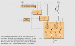
I attached TDA1541A DEM block diagram.
Ripple current is reduced on each subsequent active divider output as a result of current division. So Highest ripple current is present on bit 16 (MSB) and lowest on active divider output that feeds the 10 bit passive current divider. Ripple current also depends on tolerances in the passive divider that is part of each active divider.
Logically speaking we could halve the decoupling cap value on each subsequent active divider output. With 2uF on bit 16 we could have 1uF, 470nF, 220nF, 100nF, 47nF, and 22nF on the following active divider outputs. Something similar was already indicated in the TDA1540 data sheet:
TDA1540 datasheet pdf datenblatt - List of Unclassifed Manufacturers - 14-Bit DAC (Serial Output) ::: ALLDATASHEET :::
Also interesting to see that 10nF seems to be lowest practical value, as subsequent bits all have 10nF caps installed.
Voltage measurement suggests following active divider output to decoupling pin assignment:
Bit 16 (MSB) pins 12 & 23, bit15 pins 13 & 24, bit14, pins 11 & 22, bit13, pins 10 & 21, bit12, pins 9 & 20, bit11, pins 8 & 19, bit10, pins 7 & 18.
Listening tests however showed that equal value DEM decoupling caps offer darker background and better detail.
Is 60Khz the lowest you can go?
I am now using 22KHz (post # 4615). This is the lowest practical value, just outside the audio range and small SMD 2uF decoupling caps can be constructed by placing two 1uF 1210 size film caps in parallel. These will just fit under the IC when the IC is placed in an IC socket.
In addition I suppose the cap size would also increase to much larger levels which bring their own problems!
They would likely have much higher inductance (poorer ripple attenuation). Short PCB traces that connect the decoupling cap are already problematic. That's why the decoupling caps are best placed underneath the chip, as close to the decoupling pins and GND as possible. Electrolytic caps have both, too high inductance and too high leakage current. Note that plus of electrolytic decoupling caps would go to GND.
I remember there was someting about a divide by 2 in the thread / dem circuit notes so I guess that would still be frequencies outside of the audio band.
Since pins 16 and 17 are both inputs and outputs it is difficult to trigger / sync the circuit by external signal(s) without inducing peak currents. These peak currents increase on-chip interference and resulting jitter levels.
Is there any merit to using higher value caps on different pins? I think a few commercial manufacturers did this ? (there is a thread on it I think )
I attached TDA1541A DEM block diagram.
Ripple current is reduced on each subsequent active divider output as a result of current division. So Highest ripple current is present on bit 16 (MSB) and lowest on active divider output that feeds the 10 bit passive current divider. Ripple current also depends on tolerances in the passive divider that is part of each active divider.
Logically speaking we could halve the decoupling cap value on each subsequent active divider output. With 2uF on bit 16 we could have 1uF, 470nF, 220nF, 100nF, 47nF, and 22nF on the following active divider outputs. Something similar was already indicated in the TDA1540 data sheet:
TDA1540 datasheet pdf datenblatt - List of Unclassifed Manufacturers - 14-Bit DAC (Serial Output) ::: ALLDATASHEET :::
Also interesting to see that 10nF seems to be lowest practical value, as subsequent bits all have 10nF caps installed.
Voltage measurement suggests following active divider output to decoupling pin assignment:
Bit 16 (MSB) pins 12 & 23, bit15 pins 13 & 24, bit14, pins 11 & 22, bit13, pins 10 & 21, bit12, pins 9 & 20, bit11, pins 8 & 19, bit10, pins 7 & 18.
Listening tests however showed that equal value DEM decoupling caps offer darker background and better detail.
Attachments
Hi, oshifis
You are rule colleague. Offered by you approach is a constructive approach if prototype is discussed. But if they are discussed mathematical calculation or technical features, there is no need to build and present the prototype. It is enough to point to mistake, inexactness at calculation to insure others from repetition of the mistake.
I call this a negative attitude. A more positive attitude would be something like this:
"Look, I don't like your solution for this and this reason. It can be done better. Here is the circuit diagram, photograph, and some measurements from the prototype of my solution - which I can demonstrate is better than your approach"
You are rule colleague. Offered by you approach is a constructive approach if prototype is discussed. But if they are discussed mathematical calculation or technical features, there is no need to build and present the prototype. It is enough to point to mistake, inexactness at calculation to insure others from repetition of the mistake.
- Home
- Source & Line
- Digital Line Level
- Building the ultimate NOS DAC using TDA1541A