Simple Transimpedance for TDA1543
Hi EC,
Regarding schematic posted in Post #2540, the upper right circuit. Is it possible to use 2SK117-2SC2240 darlington instead of single 2SC2240, in order to reduce noise from base of 2SC2240? I though all output current from TDA1543 will flow through R I/V. Thanks.
Best Regards,
Art.
Hi EC,
Regarding schematic posted in Post #2540, the upper right circuit. Is it possible to use 2SK117-2SC2240 darlington instead of single 2SC2240, in order to reduce noise from base of 2SC2240? I though all output current from TDA1543 will flow through R I/V. Thanks.
Best Regards,
Art.
Hi Art,
No, this won't work, just use the 2SC2240. If you want lower noise, use multiple transistors in parallel. Also try to use (selected) transistors with highest gain.
DAC output current flows through R1, but a small current also flows through T1 (B-E). This current varies with DAC output current and T1 gain (2SC2240 gain is specified between 200 and 700).
Some examples:
iDAC = maximum (2.3mA): iB = 11.5uA (gain = 200) ... iB = 3.28uA (gain = 700).
iDAC = half (1.15mA): iB = 5.75uA (gain = 200) ... iB = 1.64uA (gain = 700).
iDAC = almost minimum (35nA): iB = 175pA (gain = 200) ... iB = 50pA (gain = 700).
The biggest problem with the trans-impedance converter is power supply noise, so make sure to use a very clean power supply.
Regarding schematic posted in Post #2540, the upper right circuit. Is it possible to use 2SK117-2SC2240 darlington instead of single 2SC2240, in order to reduce noise from base of 2SC2240? I though all output current from TDA1543 will flow through R I/V. Thanks.
No, this won't work, just use the 2SC2240. If you want lower noise, use multiple transistors in parallel. Also try to use (selected) transistors with highest gain.
DAC output current flows through R1, but a small current also flows through T1 (B-E). This current varies with DAC output current and T1 gain (2SC2240 gain is specified between 200 and 700).
Some examples:
iDAC = maximum (2.3mA): iB = 11.5uA (gain = 200) ... iB = 3.28uA (gain = 700).
iDAC = half (1.15mA): iB = 5.75uA (gain = 200) ... iB = 1.64uA (gain = 700).
iDAC = almost minimum (35nA): iB = 175pA (gain = 200) ... iB = 50pA (gain = 700).
The biggest problem with the trans-impedance converter is power supply noise, so make sure to use a very clean power supply.
Thanks for suggestion, EC. I use this circuit with 4x DI TDA1543 for few month. Supply is your charge-transfer and TeddyReg. It's far better than previously LM4562 I/V. I'll try match 2SC2240 and add to board.
Another question. I used HEF4517 for timing chain of 4X DI. Is the attenuator 3k3+3k3+1k as you suggested match the logic level.
Best Regards,
Art.
Another question. I used HEF4517 for timing chain of 4X DI. Is the attenuator 3k3+3k3+1k as you suggested match the logic level.
Best Regards,
Art.
Hi Art,
I skipped all semiconductor I/V converter / amplifier issues by using passive I/V conversion only (2 I/V resistors of 680 Ohms, a 3.2V cascaded LED reference voltage and 2 output coupling caps).
I already tested and used OP-amps like LM4562, OPA627 THS4032 and so on. They all had "issues" and are really no match for a well designed discrete circuit when it comes to resolution and micro detail in high end audio playback systems. The DAC chip outputs large bandwidth RF spectrum, and OP-amps simply can't handle this very well.
Power supply is very important for the TDA1543, LM7805 or LM317 are not very suitable if optimal performance is required (lack of micro detail and distortion).
I now use a discrete LED series regulator with integrated capacitance multiplier. The input voltage is low-pass filtered before being fed to the basis of the series regulator transistor. Most series regulator designs have the polluted input signal directly fed to the basis of the series regulator transistor.
The 3K3, 3K3, 1K attenuators are suitable for 3.3 ... 5V I2S input signal levels.
I use 5K6, 3K3 and 1K attenuators (WS and DATA only) for the SD-player. The 3K3 resistors are connected to +5V using 10mH chokes in series.
Make sure to use a dynamic jitter attenuator circuit for BCK (schematics posted on the Lossless SD-player thread).
Thanks for suggestion, EC. I use this circuit with 4x DI TDA1543 for few month. Supply is your charge-transfer and TeddyReg. It's far better than previously LM4562 I/V. I'll try match 2SC2240 and add to board.
I skipped all semiconductor I/V converter / amplifier issues by using passive I/V conversion only (2 I/V resistors of 680 Ohms, a 3.2V cascaded LED reference voltage and 2 output coupling caps).
I already tested and used OP-amps like LM4562, OPA627 THS4032 and so on. They all had "issues" and are really no match for a well designed discrete circuit when it comes to resolution and micro detail in high end audio playback systems. The DAC chip outputs large bandwidth RF spectrum, and OP-amps simply can't handle this very well.
Power supply is very important for the TDA1543, LM7805 or LM317 are not very suitable if optimal performance is required (lack of micro detail and distortion).
I now use a discrete LED series regulator with integrated capacitance multiplier. The input voltage is low-pass filtered before being fed to the basis of the series regulator transistor. Most series regulator designs have the polluted input signal directly fed to the basis of the series regulator transistor.
Another question. I used HEF4517 for timing chain of 4X DI. Is the attenuator 3k3+3k3+1k as you suggested match the logic level.
The 3K3, 3K3, 1K attenuators are suitable for 3.3 ... 5V I2S input signal levels.
I use 5K6, 3K3 and 1K attenuators (WS and DATA only) for the SD-player. The 3K3 resistors are connected to +5V using 10mH chokes in series.
Make sure to use a dynamic jitter attenuator circuit for BCK (schematics posted on the Lossless SD-player thread).
Hi ECdesigns
I am trying to make I/V output stage for pcm63 dac and tda1541a dac
would you be nice and suggest what of the follow known circuits giving best results
1. your design trans impedance http://www.diyaudio.com/forums/showthread.php?postid=1818974#post1818974
2. Jocko easy to build http://www.diyaudio.com/forums/showthread.php?postid=61496#post61496
3. Rudolf Broertjes http://www.diyaudio.com/forums/showthread.php?postid=103883#post103883
4. tschrama http://www.diyaudio.com/forums/attachment.php?postid=77793&stamp=1036433748
5. pedja OPA AD844 based (can I use NE5532 here) http://www.diyaudio.com/forums/attachment.php?s=&postid=1292141
Here is my observations.
It begins v complications and what is in ECdesign is a reduced version. The bias setting unit are later reduced. After reading the fine print, we come to the schematics as what ECdesign does here, though they dont clearly draw out the schematics. It is a IV follow by buffer.
What I have not found is the capacitor as shown in IV transimpedance and that is important.
There is another circuit using JFET to further avoid the intermodulation caused by the base current in Q1.
Simple circuit with as few components (of high quality) give good sound.
while we wait for the SD-player...
Hi,
I had the time to mod the D1M DAC replacing my 2K5 R I/V for a potentiometer: 10K bourns pot //2K5 good quality R; as "variable R" I mean legs 2 and 3 soldered to each other (saving time).
It worked OK and I took off the Pass B1 buffer.
While the solder ages... I can say the presentation is more punchy and bass is stronger, the music more involving and warm. It could be the pot though...I'll see later.
Two problems:
1) the two channels are not exactly matched so the stereo image could suffer.
-->plan to use some discrete R pots to solve this, 50K //2K good quality resistor.
2) when I go up in SPL the speaker cone make strange movements as if there were DC imbalance (or LF). If I go up very slowly there is no noise.
--> plan to make the conventional pot configuration with leg 1 (and parallel R) to ground...
EC, any advice?
Thanks,
M.
Hi,
No. Not yet. Not very much time these days to DIY...a nasty virus...
EC gave some important tips but for 5Vpp BCK:
I was thinking about searching for the right R (point #1) with a 500R pot until the desired 1volt appears across it, but I don't know if this rule still applies to lower digital signal amplitude...anyway it surely will be noticeable soundwise if it is wrong
Good luck.
M
No. Not yet. Not very much time these days to DIY...a nasty virus...
EC gave some important tips but for 5Vpp BCK:
-ecdesigns- said:Hi maxlorenz,
1) Adjust the resistor value until you measure approx. 1 volts across it. The resistor value depends on bit clock amplitude and duty cycle. With 5Vpp and exact 50% duty, R would be around 280 ... 300 Ohms.
2) Connect a scope across the resistor, make sure the circuit receives a 2.8224 MHz bit clock signal, now adjust capacitance until achieving lowest possible ripple voltage. With 300 Ohms, capacitor value would be around 100 ... 200nF.
Start with 280 Ohms and 200nF (2 x 100nF stacked foil cap in parallel).
I was thinking about searching for the right R (point #1) with a 500R pot until the desired 1volt appears across it, but I don't know if this rule still applies to lower digital signal amplitude...anyway it surely will be noticeable soundwise if it is wrong
Good luck.
M
Hi maxlorenz,
Try ALPS professional potentiometers, these have good matching.
There is a bias current running through the I/V resistor, when you (rapidly) change the value, it will cause momentary DC shifts at the DAC output as the coupling capacitor needs some time to charge / discharge to the changed DC input level.
After doing some more tests with attenuators, I settled for a 10K motorized ALPS pot, and one selectable series resistor at the speaker.
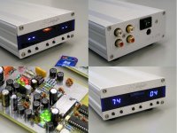
SD-player design is now completed, I attached some impressions of the finished product. This is the basic version, I also plan to design a TDA1541A-based version later, provided it offers significant better sound quality than the basic version.
1) the two channels are not exactly matched so the stereo image could suffer.
-->plan to use some discrete R pots to solve this, 50K //2K good quality resistor.
Try ALPS professional potentiometers, these have good matching.
2) when I go up in SPL the speaker cone make strange movements as if there were DC imbalance (or LF). If I go up very slowly there is no noise.
--> plan to make the conventional pot configuration with leg 1 (and parallel R) to ground...
There is a bias current running through the I/V resistor, when you (rapidly) change the value, it will cause momentary DC shifts at the DAC output as the coupling capacitor needs some time to charge / discharge to the changed DC input level.
After doing some more tests with attenuators, I settled for a 10K motorized ALPS pot, and one selectable series resistor at the speaker.
SD-player design is now completed, I attached some impressions of the finished product. This is the basic version, I also plan to design a TDA1541A-based version later, provided it offers significant better sound quality than the basic version.
Attachments
reclocking BCK with shift-register
Hi EC,
I will try the reclocking BCK using 48M (also generating 12M for PCM2706 instead of seperate oscillator), can I use following DIP package with 3.3V supply instead of SMD you used?
TI CD74AC04 (8.3ns) instead of NC7SZ04
TI CD74AC163 (73Mhz) instead of 74F163
NXP 74LV164 (78Mhz) instead of 74F164
Thanks
The I2S attenuators provide both a bias voltage (approx. 1.2V), and attenuation of the I2S signals. By lowering I2S signal amplitude, sound get's much more refined, due to reduction of I2S interference.
Hi ECDesigns,
if 2x1543 is used, can we just use one set of I2S attenuation and branch out to each of the 2 tda1543 or each set of I2S attenuation is required.
I have measure the pin at BCK, DATA, WS to be 1.8V. I guess I need to lower that to 1.2V bias.
Hi 2A3SET,
Yes, these would probably function, but 74LV164 jitter amplitude / spectrum may differ when compared with 74F164.
can I use following DIP package with 3.3V supply instead of SMD you used?
Yes, these would probably function, but 74LV164 jitter amplitude / spectrum may differ when compared with 74F164.
Hi ccschua,
It's possible to drive 2 x TDA1543 with only one set of I2S attenuators.
With TDA1543, optimal DC bias voltage (I2S inputs) equals approx. 1.2 Volts.
With 5V TTL I2S input signal amplitude, use 3K3 series resistor, 1K to GND and 3K3 to +5V (WS and DATA). For BCK use 330 Ohm series resistance, 100 Ohm to GND, and 330 Ohm to Vcc, or even better, use the BCK dynamic jitter attenuator circuit.
if 2x1543 is used, can we just use one set of I2S attenuation and branch out to each of the 2 tda1543 or each set of I2S attenuation is required.
It's possible to drive 2 x TDA1543 with only one set of I2S attenuators.
I have measure the pin at BCK, DATA, WS to be 1.8V. I guess I need to lower that to 1.2V bias.
With TDA1543, optimal DC bias voltage (I2S inputs) equals approx. 1.2 Volts.
With 5V TTL I2S input signal amplitude, use 3K3 series resistor, 1K to GND and 3K3 to +5V (WS and DATA). For BCK use 330 Ohm series resistance, 100 Ohm to GND, and 330 Ohm to Vcc, or even better, use the BCK dynamic jitter attenuator circuit.
use the BCK dynamic jitter attenuator circuit.
For 1xTDA1543 using 5V vcc and dynamic jitter attentuation circuit, I measure the BCK, WS and DATA to be 0.9V, 1.2V and 0.9V respectively. I expected all to be 1.2V. Should I change the dynamic jitter to be 1.2V for all of them ?
Nevertheless I could play with the voltage and the resolution and clarity actually improve.
- Home
- Source & Line
- Digital Line Level
- Building the ultimate NOS DAC using TDA1541A