Hi JC951t
No, the CDPROII outputs 48BCK/WS, the DI4T interpolator is designed for 64BCK/WS.
The DI4T has Toslink-only input (interference signals from the digital audio source are fully blocked).
The CDPROII can be connected through SPDIF / Toslink, this also solves the 48BCK/WS problem.
With the new dac, can it handle I2S straight from
a CD pro 2 ?
No, the CDPROII outputs 48BCK/WS, the DI4T interpolator is designed for 64BCK/WS.
The DI4T has Toslink-only input (interference signals from the digital audio source are fully blocked).
The CDPROII can be connected through SPDIF / Toslink, this also solves the 48BCK/WS problem.
Simple DAC
Hi there!
I'd like to build DIY a DAC with 1541A I found in the trash..

It comes from an old CD player 😎
I have all the peripherals componet such as the 7220 for example but I'd like a simple ne, if you feel...😀
thanks for your reply and god bless you

Hi there!
I'd like to build DIY a DAC with 1541A I found in the trash..
It comes from an old CD player 😎
I have all the peripherals componet such as the 7220 for example but I'd like a simple ne, if you feel...😀
thanks for your reply and god bless you
I2S attenuator
Dear -ecdesigns-,
Now I feel the strength to face that mod that you advice to I2S:
I have some doubts. First, following your instructions, two readings may follow. Please see the diagram.
http://picasaweb.google.com/maxlorenz24/DIDAC#5241908669720852130
Which one is good?
Second: one of the reasons to do this mod is to avoid crosstalk between I2S signals inside the DAC chip, right? But this interaction also can be produced through PCB long vias. On the other hand, it is good to have strong DATA signal to make it more resistant to noise.
Following that principles, may it be good to make the WS attenuator next to timing chain and DATA attenuator next to DAc chips? 🙂
Third: your VCC is +5V. My DI still uses +6V to power the TDA1543 DACs. Can I use it or do I have to change V or change R values?
Fourth: can I use SMD type 22R to connect BCK signal?
Many thanks,
M
Dear -ecdesigns-,
Now I feel the strength to face that mod that you advice to I2S:
You need an attenuator / level shifter for each separate TDA1543 DATA and WS input pin. So when using 4 x TDA1543, you will need 8 of these identical circuits. Put two resistors in series 3K3 to +5V, 1K to GND. The point where the two resistors are connected is your star point. The I2S DATA / WS signal is connected to this star point through another 3K3 resistor. The star point connects directly to the DAC I2S input pin. BCK is not attenuated (seems to work best), connect 4 x 22R resistor to BCK, then connect the other side of each resistor to each TDA1543 BCK input.
I have some doubts. First, following your instructions, two readings may follow. Please see the diagram.
http://picasaweb.google.com/maxlorenz24/DIDAC#5241908669720852130
Which one is good?
Second: one of the reasons to do this mod is to avoid crosstalk between I2S signals inside the DAC chip, right? But this interaction also can be produced through PCB long vias. On the other hand, it is good to have strong DATA signal to make it more resistant to noise.
Following that principles, may it be good to make the WS attenuator next to timing chain and DATA attenuator next to DAc chips? 🙂
Third: your VCC is +5V. My DI still uses +6V to power the TDA1543 DACs. Can I use it or do I have to change V or change R values?
Fourth: can I use SMD type 22R to connect BCK signal?
Many thanks,
M
Hi maxlorenz,
Fig. 1 is correct.
When connecting the I2S signals directly to the chip, the HF interference is dumped on the chip substrate, causing increased on-chip interference levels (ground-bounce & crosstalk). This interference ends-up on the DAC current outputs, and increases timing jitter.
Similar happens on a PCB, when designing a PCB for these kind of applications, same design rules apply as for RF circuits.
Data is valid or it's not. When digital audio data is corrupted, it's usually very audible (noise, drop-outs). In order to make sure I2S data integrity is always guaranteed, I applied a safety margin.
The attenuators must be placed as close as possible to the DAC chip I2S inputs. The idea is to attenuate both, the interference that's caused by the I2S signals, and the interference picked-up by the traces that carry these signals.
You can reduce it to 5V without problems, as the DI16 has an OP-amp I/V converter (ac voltage at the DAC outputs is virtually zero).
Which one is good?
Fig. 1 is correct.
Second: one of the reasons to do this mod is to avoid crosstalk between I2S signals inside the DAC chip, right? But this interaction also can be produced through PCB long vias.
When connecting the I2S signals directly to the chip, the HF interference is dumped on the chip substrate, causing increased on-chip interference levels (ground-bounce & crosstalk). This interference ends-up on the DAC current outputs, and increases timing jitter.
Similar happens on a PCB, when designing a PCB for these kind of applications, same design rules apply as for RF circuits.
On the other hand, it is good to have strong DATA signal to make it more resistant to noise.
Following that principles, may it be good to make the WS attenuator next to timing chain and DATA attenuator next to DAc chips?
Data is valid or it's not. When digital audio data is corrupted, it's usually very audible (noise, drop-outs). In order to make sure I2S data integrity is always guaranteed, I applied a safety margin.
The attenuators must be placed as close as possible to the DAC chip I2S inputs. The idea is to attenuate both, the interference that's caused by the I2S signals, and the interference picked-up by the traces that carry these signals.
Third: your VCC is +5V. My DI still uses +6V to power the TDA1543 DACs. Can I use it or do I have to change V or change R values?
You can reduce it to 5V without problems, as the DI16 has an OP-amp I/V converter (ac voltage at the DAC outputs is virtually zero).
EC, these improvements sound great
Would it be possible to convert the DI16 to passive I/V for improved SQ??
And are there any other improvements to the TDA1543 circuit you would sugest?
Cheers
Would it be possible to convert the DI16 to passive I/V for improved SQ??
And are there any other improvements to the TDA1543 circuit you would sugest?
Cheers
Hi crazy bob uk,
Yes it's possible to convert the DI16 to passive I/V conversion. I would suggest using 4 * interpolation (leave-out 12 chips).
- Lowest possible ac voltage at DAC outputs (max. I/V resistor value for 1 output approx. 221 Ohms, lower value is preferred).
- Clean 2.5V external reference voltage for passive I/V resistor reference (L-C filter).
- Clean 4.6V power supply for DAC chips (L-C filters).
- Separate power supply decoupling for each chip.
- Don't connect Vref!
- I2S attenuators.
- Damping resistors (22 ... 330R) on ALL digital outputs (timing-chain, PLL, dividers and so on).
- Lowest possible crosstalk between I2S & timing signals (PCB-routing).
- Tube or discrete all-JFET amplifiers, don't use OP-amps if you prefer best sound quality, I only use them for DC-servo now.
- Try to avoid coupling caps, one extra coupling cap is one too many. Use DC-coupling whenever possible.
These and many more improvements were used in the new DI4MJ project (based on 4 x TDA1543).
Would it be possible to convert the DI16 to passive I/V for improved SQ??
Yes it's possible to convert the DI16 to passive I/V conversion. I would suggest using 4 * interpolation (leave-out 12 chips).
And are there any other improvements to the TDA1543 circuit you would sugest?
- Lowest possible ac voltage at DAC outputs (max. I/V resistor value for 1 output approx. 221 Ohms, lower value is preferred).
- Clean 2.5V external reference voltage for passive I/V resistor reference (L-C filter).
- Clean 4.6V power supply for DAC chips (L-C filters).
- Separate power supply decoupling for each chip.
- Don't connect Vref!
- I2S attenuators.
- Damping resistors (22 ... 330R) on ALL digital outputs (timing-chain, PLL, dividers and so on).
- Lowest possible crosstalk between I2S & timing signals (PCB-routing).
- Tube or discrete all-JFET amplifiers, don't use OP-amps if you prefer best sound quality, I only use them for DC-servo now.
- Try to avoid coupling caps, one extra coupling cap is one too many. Use DC-coupling whenever possible.
These and many more improvements were used in the new DI4MJ project (based on 4 x TDA1543).
Hello,
I've been following this thread trying to understand the i2s reclocker. I want to use a pcm2706/7 to tda1541a (only one) with this reclock system. I am pretty much a noob at this so I just want to check if this works (don't mind the colours)
Is this the way I build this?
Thanks in advance
I've been following this thread trying to understand the i2s reclocker. I want to use a pcm2706/7 to tda1541a (only one) with this reclock system. I am pretty much a noob at this so I just want to check if this works (don't mind the colours)
An externally hosted image should be here but it was not working when we last tested it.
An externally hosted image should be here but it was not working when we last tested it.
Is this the way I build this?
Thanks in advance
Hi serph1nia,
Yes this should work.
U8 and U9 are shift-registers, they basically consist of 8 cascaded D flip-flops that are synchronously clocked (CLK). The output of each D flip-flop is available (QA ... QH). The first D flip-flop has 2 D inputs (AND).
Without the reset circuit (U10) it's basically a plain asynchronous reclocker (similar to two cascaded 74xx74 chips). However, this reclocker is always reset after a fixed amount of masterclock pulses (inverter Q10). So it acts as an both an asynchronous reclocker and a digital one-shot circuit. This means that the positive BCK pulse width is always fixed. The circuit requires a masterclock that oscillates at (almost) an exact multiple of BCK.
Note that the reset is asynchronous here, I later improved this circuit by not using the reset inputs (tied to VCC), and feeding QH (U8) back to the second D flip-flop input (B) of U8, using inverter U10, B needs to be disconnected from input A of course.
This is basically an asynchronous reclocker that changes the jitter frequency spectrum, but doesn't block it.
I think it's best to drive the DAC chips directly from a (2.8224 MHz) masterclock, without any reclocking. This requires synchronization between both source and masterclock.
I've been following this thread trying to understand the i2s reclocker. I want to use a pcm2706/7 to tda1541a (only one) with this reclock system. I am pretty much a noob at this so I just want to check if this works (don't mind the colours)
Yes this should work.
U8 and U9 are shift-registers, they basically consist of 8 cascaded D flip-flops that are synchronously clocked (CLK). The output of each D flip-flop is available (QA ... QH). The first D flip-flop has 2 D inputs (AND).
Without the reset circuit (U10) it's basically a plain asynchronous reclocker (similar to two cascaded 74xx74 chips). However, this reclocker is always reset after a fixed amount of masterclock pulses (inverter Q10). So it acts as an both an asynchronous reclocker and a digital one-shot circuit. This means that the positive BCK pulse width is always fixed. The circuit requires a masterclock that oscillates at (almost) an exact multiple of BCK.
Note that the reset is asynchronous here, I later improved this circuit by not using the reset inputs (tied to VCC), and feeding QH (U8) back to the second D flip-flop input (B) of U8, using inverter U10, B needs to be disconnected from input A of course.
This is basically an asynchronous reclocker that changes the jitter frequency spectrum, but doesn't block it.
I think it's best to drive the DAC chips directly from a (2.8224 MHz) masterclock, without any reclocking. This requires synchronization between both source and masterclock.
Hi ec design
could You post the sch of the
improved I2S attenuators please?
I would like to try...
could You post the sch of the
improved I2S attenuators please?
I would like to try...
Hi Zoran,
1K5 resistor close to WS / DATA outputs (primary series resistor).
PCB trace or wire from 1K5 to the attenuator.
Attenuator:
Input to VCC using 3K3 (pull-up resistor).
Input to GND using 1K0 (pull-down resistor).
Input to trace 1K8 (secondary series resistor, close to DAC chip input).
BCK, only series resistor:
TDA1543, 330R.
TDA1541A, 22R.
There are many other options to boost TDA1543 / TDA1541A performance.
One big problem seems to be L / R channel tolerances, Bernhard already documented this with measurements. Both channels are located on specific spots on the chip, and are surrounded by different circuits, so each channel has a unique noise frequency spectrum. When the same channels are paralleled (L+L+L+L ... R+R+R+R) errors are correlated, and might prevent correct averaging of bit errors.
So paralleling multiple DAC chips "the easy way" might even lead to increased distortion.
One way to prevent this, is swapping L/R channels inside the DAC chip. This can be done by manipulating the serial I2S data for half of the paralleled DAC chips. This also means that the L/R outputs on these chips need to be swapped!
Yesterday I designed, built and tested a scrambler / interpolator circuit for the DI4T. This circuit swaps L/R channels on 2 chips in order to prevent errors due to correlation, provides the required delays for interpolation, and inverts the data for 2 chips. I added a picture of the scrambler / interpolator prototype being tested on the DI4T. It only consists of 4 standard logic chips. I2S enters on the left (BCK, WS and DATA), and is split-up in separate WS and DATA signals for each DAC chip.
The scrambler / interpolator was designed to provide balanced output signals and 4 x interpolation:
DAC #1, L16 / R16 (channels delayed).
DAC #2, NR48 / NL48 (channels swapped, delayed and inverted).
DAC #3, L32 / R32 (channels delayed).
DAC #4, NR64 / NL64 (channels swapped, delayed and inverted).
Now the L / R channel on-chip tolerances are correctly averaged. This doesn't seem to be that spectacular until you hear the results.
Attachments

Hi ec design
I've been following this thread and have learned a lot.
I am looking for solution to connect computer to DAC. Using Toslink to isolate interference is good idea. However, I have read that the rise and fall times of the LED and photodiode are asymmetric. Also, the interface will introduce a peak-to-peak jitter equal to the pulse length error.
Are there any Toslink Transmitter and receiver have better spec to avoid those issues? Do i need special care to connect toslink cable to the Transmitter and receiver?
best regard
wing
Hi wingwing,
I only use Toslink for data transfer, so wideband jitter of a few thousand picoseconds rms is no problem at all, as long as no data corruption occurs. Average Toslink jitter is well below the critical value that causes data corruption.
I am now testing a micro-controller based precision tracker in both DI4MJ and DI4T. It basically consists of a small microcontroller that measures both source and PXO (Programmable Crystal Oscillator) frequency, and matches the PXO frequency by using a 10-bit code. This results in 0.19ppm step accuracy. Only one correction is allowed every 2 seconds, this puts the "corner frequency" of the tracker at 0.5Hz.
The SPDIF (Toslink) receiver runs in slave-clock mode (both WS and BCK are set as input).
if the connected DAC is sensitive to source jitter, every single part in the optical circuit could affect sound quality. In this case one could use real glass-fibre interlinks that have an optical core that consists of multiple thin strands.
Modern SPDIF receivers like CS8416 have 3.3V power supply, in order to prevent over-driving the SPDIF inputs, a 3.3V optical receiver (RX147L) must be used. It's also advisable to attenuate the output signal using a 1K / 330R resistive attenuator.
The modern Toslink receivers like RX147L and RX177L have larger bandwidth (faster switching) and are preferred.
I have read that the rise and fall times of the LED and photodiode are asymmetric. Also, the interface will introduce a peak-to-peak jitter equal to the pulse length error.
I only use Toslink for data transfer, so wideband jitter of a few thousand picoseconds rms is no problem at all, as long as no data corruption occurs. Average Toslink jitter is well below the critical value that causes data corruption.
I am now testing a micro-controller based precision tracker in both DI4MJ and DI4T. It basically consists of a small microcontroller that measures both source and PXO (Programmable Crystal Oscillator) frequency, and matches the PXO frequency by using a 10-bit code. This results in 0.19ppm step accuracy. Only one correction is allowed every 2 seconds, this puts the "corner frequency" of the tracker at 0.5Hz.
The SPDIF (Toslink) receiver runs in slave-clock mode (both WS and BCK are set as input).
Are there any Toslink Transmitter and receiver have better spec to avoid those issues? Do i need special care to connect toslink cable to the Transmitter and receiver?
if the connected DAC is sensitive to source jitter, every single part in the optical circuit could affect sound quality. In this case one could use real glass-fibre interlinks that have an optical core that consists of multiple thin strands.
Modern SPDIF receivers like CS8416 have 3.3V power supply, in order to prevent over-driving the SPDIF inputs, a 3.3V optical receiver (RX147L) must be used. It's also advisable to attenuate the output signal using a 1K / 330R resistive attenuator.
The modern Toslink receivers like RX147L and RX177L have larger bandwidth (faster switching) and are preferred.
Hi -ECdesigns- 🙂
That's what discourages me: you do in one day what will take me a month to plan and build... 🙁
I understand but with a diagram it could be easier...
So, with TDA1543 a 330R is better on BCK signal...OK, I have time to correct it.
Cheers,
M
Yesterday I designed, built and tested a scrambler / interpolator circuit for the DI4T.
That's what discourages me: you do in one day what will take me a month to plan and build... 🙁
The scrambler / interpolator was designed to provide balanced output signals and 4 x interpolation: DAC #1, L16 / R16 (channels delayed). DAC #2, NR48 / NL48 (channels swapped, delayed and inverted). DAC #3, L32 / R32 (channels delayed). DAC #4, NR64 / NL64 (channels swapped, delayed and inverted). Now the L / R channel on-chip tolerances are correctly averaged. This doesn't seem to be that spectacular until you hear the results.
I understand but with a diagram it could be easier...
So, with TDA1543 a 330R is better on BCK signal...OK, I have time to correct it.
Cheers,
M

-ecdesigns- said:One big problem seems to be L / R channel tolerances, Bernhard already documented this with measurements. Both channels are located on specific spots on the chip, and are surrounded by different circuits, so each channel has a unique noise frequency spectrum. When the same channels are paralleled (L+L+L+L ... R+R+R+R) errors are correlated, and might prevent correct averaging of bit errors.
IIRC, in Philips players, with os always the same channel had more LL distortion than the other.
But there were a few exceptions where the other channel was better.
Also IIRC the 1541A with 7220A had a characteristic spectrum around K5 & K7, which changed to K2 K4 K6 K8 with nonos.
IMHO in both cases the characteristic spectrum = sine waveform means that paralleling chips does not average out any errors.
I had put 3 TDAs in parallel without success.
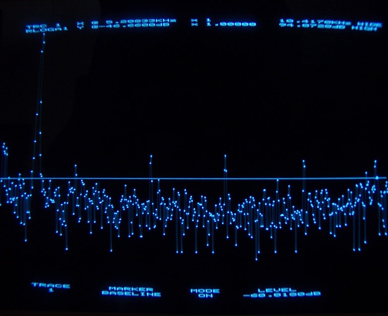
Old picture of 1541A nonos:
maybe it is not about the distorsion...
but i check 1, 8, 16 tda1543 in parallel, at the same system
and winner is 16...
with instantly noticable sound improvement
and I was not alone in that test, everybody was reacted on the same way.
*
So maybe it is issue of rapid decrease of output impedance?
And linearising in highs was much better then 1 chip, no need for corrections
*
ecdesigns,
Thanks a lot for your reply.
Thanks a lot for your reply.
This is what I love to see. I guess it is similar to Lavry's CystalLock. http://www.lavryengineering.com/white_papers/DA924m.pdf-ecdesigns- said:Hi wingwing,
I am now testing a micro-controller based precision tracker in both DI4MJ and DI4T. It basically consists of a small microcontroller that measures both source and PXO (Programmable Crystal Oscillator) frequency, and matches the PXO frequency by using a 10-bit code. This results in 0.19ppm step accuracy. Only one correction is allowed every 2 seconds, this puts the "corner frequency" of the tracker at 0.5Hz.
- Home
- Source & Line
- Digital Line Level
- Building the ultimate NOS DAC using TDA1541A