Also, and I'm just mentioning this because it is a practical issue, if there is any oxidation on component leads and so on then that can prevent a true voltage reading. Really push the probe hard onto the components (but mind you don't slip with them) to be absolutely certain of the readings.
Remember what you said about never believing the customer?
I still hadn't confirmed the "no sound" report from mine. Turns out there is, in fact, sound. The sine wave passed through, as did music. The only anomaly I noted was that the sine wave at the speaker terminal on the right side was actually not as clean as the one on the left.
I still hadn't confirmed the "no sound" report from mine. Turns out there is, in fact, sound. The sine wave passed through, as did music. The only anomaly I noted was that the sine wave at the speaker terminal on the right side was actually not as clean as the one on the left.
Also, and I'm just mentioning this because it is a practical issue, if there is any oxidation on component leads and so on then that can prevent a true voltage reading. Really push the probe hard onto the components (but mind you don't slip with them) to be absolutely certain of the readings.
Understood. I rechecked the previous voltage measurements between the gates, and they're all the same.
Remember what you said about never believing the customer?
Oh yes. I've been there a zillion times
")
So we do have sound. That leaves the rather strange problem of the weird readings and no bias which would account for the distortion (crossover distortion).
I'm going to say that our theory is good and will hold up under scrutiny, and so that means that if you have 1.23 volts across a pair of FET gates (as measured on the pins of the FET (not just the sockets), and the rail voltage to those FET's is correct (as measured on the FET itself), and that the 0.22 ohms are good and go where they are supposed to (actually connect to the pins of FET) and you have no bias current flowing in that pair of FET's then they have to be faulty.
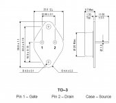
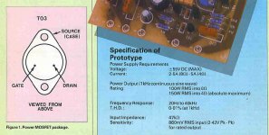
If everything connection wise checks out then we have to be looking at the FET's. Here are the data sheets. The 'Source' of each FET is the case, and so the case should be the terminal in contact with the 0.22 ohms. The Drain should have + supply present for the 2SK devices and - supply present for the 2SJ's
Make sure the gate connections are correct. Would it even survive if they were not
You have to check though... and as I might have said somewhere... never assume anything to be correct until proved to be so.
Attachments
Oh yes. I've been there a zillion times
So we do have sound. That leaves the rather strange problem of the weird readings and no bias which would account for the distortion (crossover distortion).
I'm going to say that our theory is good and will hold up under scrutiny, and so that means that if you have 1.23 volts across a pair of FET gates (as measured on the pins of the FET (not just the sockets), and the rail voltage to those FET's is correct (as measured on the FET itself), and that the 0.22 ohms are good and go where they are supposed to (actually connect to the pins of FET) and you have no bias current flowing in that pair of FET's then they have to be faulty.
If everything connection wise checks out then we have to be looking at the FET's. Here are the data sheets. The 'Source' of each FET is the case, and so the case should be the terminal in contact with the 0.22 ohms. The Drain should have + supply present for the 2SK devices and - supply present for the 2SJ's
Make sure the gate connections are correct. Would it even survive if they were not
You have to check though... and as I might have said somewhere... never assume anything to be correct until proved to be so.
Hmmm... So going over the connections again, I saw something. I need you to check me on this.
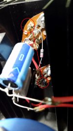
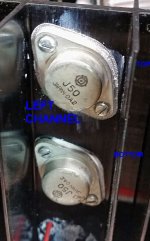
It concerns the orientation of the left bottom J50 (and subsequent connections) compared to that of the right bottom J50. In the first attached photo of the right pair of J50s, you can see that the bottom one is oriented upside down compared to the top one. And, as you'd expect the connections on the other side are opposite as well. The socket terminal for the top gate is at 12 o'clock, whereas it's at 6 o'clock on the bottom. The 220 ohm resistors are correctly wired between them.
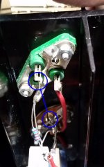
The left bottom J50 is also flipped upside down. In this case, the top J50 gate terminal is at 12 o'clock, but the bottom "gate" terminal is not at 6 o'clock as it should be, but also at 12 o'clock. So it seems that the top gate is actually wired with the 220 ohm resistors to the bottom drain, and the bottom gate is connected to the top drain.
Now this all assumes that the printing on the back of the transistor has any relation to the orientation of the pins. If it doesn't, then just ignore everything I wrote, But if it does....
Attachments

The printing normally would be similar (as far as I know) but you identify the leads by the fact the package isn't symmetrical, the two pins are away from the centre line of the package (see attached image above). That's not easy to determine from the pictures of the sockets. You might be able to judge that better by looking at different angles.
You're right. I forgot to mention that I did look at the positioning of the pins with respect to the center line. Viewed from the socket side (the only thing I have to go by until I pull the FET), the leads are connected to the correct terminals. But IF the printing on the case in relation to the pins is the same as the other three J50s, then the orientation is reversed. I'm going to remove the FET to check (annoying that it requires desoldering the pins), but if true, would this explain the strange readings?
Ok, after reorienting the left bottom J50 (F in the diagram from Mooly), I checked the gate voltages again. They are the same as before. Sigh.
So we are squarely back to replacing a faulty pair of FETs. Am I correct in assuming (there's that word again!) that it would be C and D? The voltage across their gates was +0.77V, rather than the +1.23 it was supposed to be. The drain of C (K135) has the correct + supply and the drain of D (J50) has the correct - supply. For the 220 ohm resistors, they all measure 220 ohms in circuit, with one exception: the resistor coming from the gate of D. It measures 200 ohms. I actually replaced this resistor once because it read low (200 ohms) in circuit but was 220 ohm when removed and measured again. Seems odd that the other three would measure correctly without lifting one end, but not this one that's connected to the problem FET.
So we are squarely back to replacing a faulty pair of FETs. Am I correct in assuming (there's that word again!) that it would be C and D? The voltage across their gates was +0.77V, rather than the +1.23 it was supposed to be. The drain of C (K135) has the correct + supply and the drain of D (J50) has the correct - supply. For the 220 ohm resistors, they all measure 220 ohms in circuit, with one exception: the resistor coming from the gate of D. It measures 200 ohms. I actually replaced this resistor once because it read low (200 ohms) in circuit but was 220 ohm when removed and measured again. Seems odd that the other three would measure correctly without lifting one end, but not this one that's connected to the problem FET.
If we are down to replacing FET's then I would definitely begin by removing all four from the channel being worked on and then begin replacement with a single pair only and make sure that works as expected and that it biases up correctly. When that is proved good, fit the second pair.
Also before fitting the replacements, be sure to set the bias voltage (voltage across the 150 ohm) to minimum.
This also seems a good time to get rid of those sockets and mount the FET's conventionally.
The originals are obsolete these days but alternatives exist. These are listed as replacements for the old 2SK/2SJ devices.
ECF10N20 - Metal Lateral MOSFET
ECF10P20 - Metal Lateral MOSFET
what I would try
dbxdx5
If the gate resistor shows a different reading, then the gate maybe damaged. What I would do is lift the suspected fet's gate wire, short gate to case (source) effectively taking it out of the circuit, without removing it from the socket and see if amp bias works correctly now, with one output device. It doesn't look like the gate is "shorted" to drain.
My 2 cents,
Mad
Remember each FET has its own 220 ohm gate stopper. The critical voltage is that over the 150 ohm and that voltage is high enough to bias each FET pair (assuming good and correctly wired FET's).
A gate failure might reasonably be assumed to interfere with things... but the 150 ohm voltage says otherwise. It is present and correct.
Although any voltage dropped across a 220 ohm due to a faulty gate is pulling current from the drivers, it isn't pulling the required bias voltage down.
A gate failure might reasonably be assumed to interfere with things... but the 150 ohm voltage says otherwise. It is present and correct.
Although any voltage dropped across a 220 ohm due to a faulty gate is pulling current from the drivers, it isn't pulling the required bias voltage down.
If we are down to replacing FET's then I would definitely begin by removing all four from the channel being worked on and then begin replacement with a single pair only and make sure that works as expected and that it biases up correctly. When that is proved good, fit the second pair.
Also before fitting the replacements, be sure to set the bias voltage (voltage across the 150 ohm) to minimum.
This also seems a good time to get rid of those sockets and mount the FET's conventionally.
The originals are obsolete these days but alternatives exist. These are listed as replacements for the old 2SK/2SJ devices.
ECF10N20 - Metal Lateral MOSFET
ECF10P20 - Metal Lateral MOSFET
Thanks.
I'm going to do ONE more check of everything before I go ahead and order the new FETs.
Few questions:
1. Could the reversed J50 I found caused one or more FETs to fail? Given how robust everyone says lateral FETs are, I'm concerned that whatever caused this failure could also damage the new ones if I don't ID the original cause.
2. What TO-3 sockets are recommended in lieu of what's currently in there?
3. Is there any reason to choose the Exicon replacements over those being offered by Trollet? His are matched, and I don't believe the Exicons are.
The Exicons are the current generation of lateral FET but Trollets offerings should be fine.
I've never used T03 sockets and so wouldn't know is available tbh. I'd be starting from scratch searching.
As to what has happened to this amp and the FET's, well that's open to speculation. These device are moderately static sensitive and so basic precautions should be used when handling them... no running on a nylon carpet and then grabbing hold of them, that kind of thing.
They do have inbuilt Zener diode protection on the gates and I wouldn't like to speculate on what incorrectly wiring one up would actually do.
Your amp plays, the bias control voltage adjusts OK and so I think you have to take the step of fitting new devices (just one pair at first though) and confirm all is good. A single pair is good for around 70 watts rms output and they really are tough when used correctly.
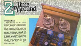
Have a look at the specs for this one... single pair of transistors. It was classic design and highly rated at the time (and still is).
I've never used T03 sockets and so wouldn't know is available tbh. I'd be starting from scratch searching.
As to what has happened to this amp and the FET's, well that's open to speculation. These device are moderately static sensitive and so basic precautions should be used when handling them... no running on a nylon carpet and then grabbing hold of them, that kind of thing.
They do have inbuilt Zener diode protection on the gates and I wouldn't like to speculate on what incorrectly wiring one up would actually do.
Your amp plays, the bias control voltage adjusts OK and so I think you have to take the step of fitting new devices (just one pair at first though) and confirm all is good. A single pair is good for around 70 watts rms output and they really are tough when used correctly.
Have a look at the specs for this one... single pair of transistors. It was classic design and highly rated at the time (and still is).
Attachments
I don't know what test equipment you have available but the FET's could be tested out of circuit in a simple DC test set up. Basically connecting the FET across a power source (power supply, battery etc) with a small load in series with the drain. A preset pot to swing the gate voltage would confirm if the FET conducted or not and at what sort of voltages.
- Status
- This old topic is closed. If you want to reopen this topic, contact a moderator using the "Report Post" button.
- Home
- Amplifiers
- Solid State
- Borbely DC 100 Amp: Left Channel Troubleshooting