at audio frequencies plane currents are largely "resistance" controlled and do not "voluntarily" form mag field minimizing "image" currents under traces that make gnd/power planes so useful with high speed digital
driver and output devices really need dedicated, purpose designed power distribution to make the current/return loop paths as balanced "common centroid" as possible if you want to minimize radiated mag field from the more nonlinear currents - particularly with Class AB/B output
you also don’t want the nonlinear current returns completing by flowing across your clean front end gnd plane and giving common impedance coupling
way too many layouts posted here have +/- power entering from opposite edges of the boards - very wrong! - they should enter the board, be routed as close together as possible (with the possible exception of floating, independant secondary dual supplies where you can twist each power with its own return)
parasitic C from power planes may reduce PSRR at some points in the circuit - I definitely section/split, leave voids, and do "fat" power trace routing in my power layer in strain gage instrumentation boards - I have 8000x amplification, 16 bit ADC and 40 MHz DSP all running with in a few inches of each other on a single board
I have also seen too many simplistic "star gnd" layouts - I think about the current loops, and often have a "hierarchy" of gnd - with front end analog gnd often a plane but splits/slots define the branch to "dirty gnd" to keep large nonlinear (noisy digital mostly in my instrumentation) currents from "diffusing" into/across my clean analog gnd - and only flitered power should be routed over the clean gnd
Hi jcx,
These are all very good points. I like to say "follow the currents" and try to be intentional about the path they take. The point about the nonlinear class AB output stage currents cannot be emphasized enough. As you point out, the +/- rails need to be close together to cancel out the magnetic fields to the extent possible, and we must try to take advantage of the fact that the sum of the +/- rail currents is a fairly linear representation of the signal.
In that same regard, I see many amplifiers where all of the PNP output devices are grouped together and all of the NPN output devices grouped together. This makes it much more difficult to get the nonlinear magnetic fields to cancel to the extent possible. I prefer to interleave the PNP and NPN output transistors and try to get the currents to circulate locally to the extent possible.
For power and ground, I like to think in terms of islands rather than planes most of the time. Of course there are exceptions, but it is not always optimal to just dedicate one whole layer to a single big plane.
Your words about the star ground are also right on. The star ground is an important concept but it does not always solve all of the problems. I am a big fan of star-on-star arrangements. Again, we need to focus on where and how the currents flow and that even though the resistances in ground and supplies are typically small, the current will still take the lowest-resistance path. It is also important to recognize that the "star" in most power amplifiers is not necessarily equi-potential and that it is not the best choice to have very high currents flowing through it. For example, I like to sum and resolve the high-current rectifier spikes in a separate node before connecting that to the star ground with a single wire. I don't want those high, spikey currents flowing in my star ground.
Cheers,
Bob
This discussion is very insightful, I like Bob 'interleaving concept', I should use it in my next PCB !!
Cheers
Arturo
Hi Artu,
I'm glad you're finding this turn of the discussion helpful. The nasty "half-wave" output stage currents in class AB amplifiers can be a real problem and can lead to sensitivities to layout details we might not have anticipated.
I've never looked deeply into this, but at times I have wondered if one of the benefits in sound quality that class A amps sometimes enjoy might be due to the relative absence of these nonlinear currents in the amplifier.
Cheers,
Bob
Hi Bob,
I've really been enjoying trying your simulations, messing around with them and then going back to the book to read the theory again. If you like you can have a look on my thread "a different CAS typology".
As I'm now looking at noise, I remember reading that you were working to improve the noise simulation accuracy of your models. Are the current models on your web site updated to include this work?
Thanks again for the great book and all the simulation examples and models, it's quite invaluable for folks like myself.
Regards,
Ken
FR4
Hi Bob,
I am a bit late to get back to you ( I just became dady for the first time ! ).
Indeed I use improved FR4 (www.eurocircuits.com) - However I have no clue what that 'improved' means. Thickness 1.55mm - inner layers are 35um Cu, outer layers are 17.5um Cu.
In my next PCB I want to concentrate on getting some tracks very short.
I used to think large = safer = better etc. Large tracks, spacefull PCB, large resistots CMF65 Vishay, largely Heatsinked VAS transistors, very large Capacitors... I thought the only drawback was cost, and that I was willing to accept.
However that way I ended up with very very large PCB surfaces, very very long tracks (up to 30 cm), ...
This time I wil go for 250mW or less resistors there where it is possible. I will choose to use a resistor power rate always over double the simulated power but not more. I ban all heatsinking in IPS and VAS, if necessary I wil lower quiescent currents to remain within half the Pd of the Q's w/o Heatsink.
Capacitor values will be limited for zener refs to 47uF whereas it used to be 100uF up to 470uF.
I noticed also on some pictures that the IPS ltp Q's are tyrapped together (it's easy with TO92 cases) for thermal compensation. Looks interesting and complies with the idea of keeping all close together.
Before sending it to manufacturing I would like you guys to have the most critical look at it . This might take a few weeks however...
Ciao for now guys,
Olivier
Hi Bob,
I am a bit late to get back to you ( I just became dady for the first time ! ).
Indeed I use improved FR4 (www.eurocircuits.com) - However I have no clue what that 'improved' means. Thickness 1.55mm - inner layers are 35um Cu, outer layers are 17.5um Cu.
In my next PCB I want to concentrate on getting some tracks very short.
I used to think large = safer = better etc. Large tracks, spacefull PCB, large resistots CMF65 Vishay, largely Heatsinked VAS transistors, very large Capacitors... I thought the only drawback was cost, and that I was willing to accept.
However that way I ended up with very very large PCB surfaces, very very long tracks (up to 30 cm), ...
This time I wil go for 250mW or less resistors there where it is possible. I will choose to use a resistor power rate always over double the simulated power but not more. I ban all heatsinking in IPS and VAS, if necessary I wil lower quiescent currents to remain within half the Pd of the Q's w/o Heatsink.
Capacitor values will be limited for zener refs to 47uF whereas it used to be 100uF up to 470uF.
I noticed also on some pictures that the IPS ltp Q's are tyrapped together (it's easy with TO92 cases) for thermal compensation. Looks interesting and complies with the idea of keeping all close together.
Before sending it to manufacturing I would like you guys to have the most critical look at it
. This might take a few weeks however...Ciao for now guys,
Olivier
"As you point out, the +/- rails need to be close together to cancel out the magnetic fields to the extent possible, and we must try to take advantage of the fact that the sum of the +/- rail currents is a fairly linear representation of the signal."
If we are talking a class AB amp here - in principle (lets ignore the class A part of the class AB bit), current is either flowing from V+ through the pass transistor, the load and then 0V OR it flowing from V- back to 0V via the lower pass transistor and the load. Although the currents from both the V+ and V- lines sum to closely approximate the load current, they do so in half cycles. Thus, wiring the the + and - supplies close together wont help.
Am I missing something here?
yes.the currents from both the V+ and V- lines sum to closely approximate the load current, they do so in half cycles. Thus, wiring the the + and - supplies close together wont help.
Am I missing something here?
The return for the two half cycles is the Zero Volts wire.
The +ve & -ve & 0V are brought to the board as a triplet.
This triplet should continue as a low radiating triplet (small loop area) to the high current consumers (Output devices and probably Drivers).
Hi Bob,
I've really been enjoying trying your simulations, messing around with them and then going back to the book to read the theory again. If you like you can have a look on my thread "a different CAS typology".
As I'm now looking at noise, I remember reading that you were working to improve the noise simulation accuracy of your models. Are the current models on your web site updated to include this work?
Thanks again for the great book and all the simulation examples and models, it's quite invaluable for folks like myself.
Regards,
Ken
Hi Ken,
I'm glad you're enjoying the simulations. I hope to have more simulations posted soon.
The current transistor models on the web page have not yet been updated to include better noise parameters, as dictated by RB. I'm working to get these put up very soon, along with models of several additional transistors.
Most of the small-signal transistor models on the site right now reflect the manufacturers' numbers for RB, which in most cases are way off and way optimistic, so noise results you get right now will probably be optimistic.
Inferring an estimate of RB for SPICE models is difficult and involves compromizes. DC measurements often do not yield reliable numbers for RB on small-signal devices. I have been doing it by making actual noise measurements with the real transistors at a typical operating point.
Cheers,
Bob
Hi Bob,
I received your book today, and I am starting to read and enjoy it.
You did not coment on the TRIPLET with TT tranistors I presented in #1506 and #1509.
I understand that you do not have time to look in every qustion, but I still hoped.
Now I have to find all answers from the book.
Damir
I received your book today, and I am starting to read and enjoy it.
You did not coment on the TRIPLET with TT tranistors I presented in #1506 and #1509.
I understand that you do not have time to look in every qustion, but I still hoped.
Now I have to find all answers from the book.
Damir
not Bob, but I can run a sim, have read a little about amp design...
rather odd choice of bias current - I would expect with the VAS ~10 mA the buffer/pre-driver of the triple to be at least several times higher than that - you have ~2 mA there - little wonder you see no improvement with the triple!
R24 I expect does nothing - at 330K and connected to 1K that is bootstrapped to ~90% of its V I don't see how it can have much effect - in AC gnded 2-pole it would put a limit on low frequency loop gain if the Q parasitics didn't limit it 1st
random comment:
R18 collector R gives some Miller multiplication and should be Zener or C shunted/bypassed if you need the V drop or current limit
Hi Bob,
I received your book today, and I am starting to read and enjoy it.
You did not coment on the TRIPLET with TT tranistors I presented in #1506 and #1509.
I understand that you do not have time to look in every qustion, but I still hoped.
Now I have to find all answers from the book.
Damir
rather odd choice of bias current - I would expect with the VAS ~10 mA the buffer/pre-driver of the triple to be at least several times higher than that - you have ~2 mA there - little wonder you see no improvement with the triple!
R24 I expect does nothing - at 330K and connected to 1K that is bootstrapped to ~90% of its V I don't see how it can have much effect - in AC gnded 2-pole it would put a limit on low frequency loop gain if the Q parasitics didn't limit it 1st
random comment:
R18 collector R gives some Miller multiplication and should be Zener or C shunted/bypassed if you need the V drop or current limit
Thank you jcx for your coment.
You say that it odd choice of bias current. The less predriver load on VAS is better, isn't it?
Triple I used was suggested by Bob in Thermaltrak tread and I changed it a little.
Regarding R18 it is for beta enhancemet BJT protection. It happens that in some transient condition Q7 could be burned. Haw you will do that? Can you show a diagram?
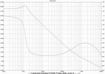
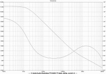
R24 makes OLG looks better, no 8dB bump on amplitude graph and phase is a bit better.
I appreciate your help here.
I will try to change the currents in predriver and see if it helps.
Graphs are without and with R24.
dado
Attachments
Hi Bob,
I received your book today, and I am starting to read and enjoy it.
You did not coment on the TRIPLET with TT tranistors I presented in #1506 and #1509.
I understand that you do not have time to look in every qustion, but I still hoped.
Now I have to find all answers from the book.
Damir
Hi Damir,
I apologize for not getting back to you on that amplifier circuit. You've got a lot going on there.
I normally recommend caution in regard to the type of circuit you are using to bootstrap the input cascodes; I'm not crazy about injecting extra current into the LTP tail circuit. I might have used an emitter follower into whose emitter I would have flowed that current. I prefer the driven cascode that is driven by a replica of the feedback signal, which, under normal conditions, is pretty much the same as the common mode signal.
Your capacitor C7 is curious, and could seem to create a noisy VAS bias current, since C7 straddles the power rails.
The ThermalTrak biasing circuit is interesting and requires some thought, but how do you adjust the bias? Am I missing something here?
Cheers,
Bob
Hi Bob,
I saw this from you in the Douglas Self thread:
I must be doing something wrong, using your models and noise example I get the following for your Figure 3.10. Help!
Thanks
I saw this from you in the Douglas Self thread:
For example, the feedback network shunt resistor is often the biggest contributor if the feedback network resistance values are not kept very low (500 ohms or less). Also, any power amplifier whose input-referred noise is less than about 10 nV/rt Hz is already quite exceptional in the noise department given the line level signals present at the input. In my amplifier of my book Figure 3.8, input-referred noise using a 200 ohm NFB network is 6.5 nV/rt Hz using 470 ohm current mirror degeneration resistors and drops to 5.7 nV/rt Hz using 1k current mirror degeneration resistors. Nevertheless, if one can pick up a couple of dB by just a modest increase in the current mirror degeneration resistors that is a good thing.
Cheers,
Bob
I must be doing something wrong, using your models and noise example I get the following for your Figure 3.10. Help!
Thanks
Attachments
Hi Damir,
I apologize for not getting back to you on that amplifier circuit. You've got a lot going on there.
I normally recommend caution in regard to the type of circuit you are using to bootstrap the input cascodes; I'm not crazy about injecting extra current into the LTP tail circuit. I might have used an emitter follower into whose emitter I would have flowed that current. I prefer the driven cascode that is driven by a replica of the feedback signal, which, under normal conditions, is pretty much the same as the common mode signal.
Your capacitor C7 is curious, and could seem to create a noisy VAS bias current, since C7 straddles the power rails.
The ThermalTrak biasing circuit is interesting and requires some thought, but how do you adjust the bias? Am I missing something here?
Cheers,
Bob
Hi Bob,
Thank you for your comments.
I wanted to keep drain - source valtage constant. Luxman amp did it simple with resistor devider. Roender is using something similar in his one stage amp.
I don't understand what you mean by using emitter follower. How to connect it to feedback signal? If you could put some diagram here, as I did not find, how to best bias a cascode, in your book.
C7 is suggested by Samuel Groner in his comment on D.Self. It enhace slew rate. And indeed in my simulation it increased dow slope from cca 70V/us to cca 90V/us. http://www.diyaudio.com/forums/soli...r-amplifier-design-handbook-douglas-self.html
R42 is used to adjust the bias. I used your suggestion for ThermalTrak from the tread http://www.diyaudio.com/forums/soli...n-thermal-trak-transistors-2.html#post1265193
I included a new LTSpice with simpler cascode bias, TTP tail current of 6mA.
Damir
Attachments
Hi Bob,
I saw this from you in the Douglas Self thread:
I must be doing something wrong, using your models and noise example I get the following for your Figure 3.10. Help!
Thanks
Hi klewis,
You are seeing about 147 nV/rt Hz at the output of the amplifier. You must refer it to the input by dividing that number by the closed-loop gain, which is about 20, yielding about 7 nV/rt Hz.
Cheers,
Bob
Carlos raised the following question over on Samuel Groner's thread concerning comments about Doug Self's book:
This is an old question and touches on numerous mis-understandings and paradoxes. I have touched on some of this in my book.
This question is also related to the question: why do some amplifiers that measure well on the test bench sound not so good?
The short answer is that extremely low distortion, as measured by conventional lab techniques like THD+N, is neither necessary nor sufficient to create an amplifier with very good sound quality as perceived by the listener.
That statement from a guy like me should get your attention.
First paradox: else why do some tube amplifiers sound very good? Their distortion taken as a lump is larger, but the nature of the distortion may be different; e.g., lower order.
The first question is whether we are talking about 1 kHz THD or 20 kHz THD? The former is nearly worthless as a measure, and is relatively easy to achieve in even a relatively crappy amplifier.
Assuming it is 20 kHz THD, over what measurement bandwidth are we measuring it, and are we taking into account the greater importance of higher harmonics? The same THD composed of only seconds and thirds will sound much more benign than the same distortion amount with significant energy at high harmonics out to the 5th, 7th, 9th etc.
Recognize that the badness of distortion we hear is usually the intermodulation products, not the harmonics. This destroys the argument that some make that we cannot hear harmonics above 20 kHz.
Recognize that distortion like 20 kHz THD is a symptom of a lack of linearity, and linearity is what we seek, including in the open loop.
Comparing amplifier distortion to loudspeaker distortion is rather meaningless, since speaker distortion is more of a soft, more benign nature, mostly low-order. Moreover, louspeakers that are 2-way and 3-way have crossovers that tend to prevent the formation of some of the IM products.
Crossover distortion is a major menace to sound quality in class AB amplifiers. For this reason, statements about distortion must include the full range of power output, in some cases to below the noise floor of the THD analyzer. When you read a review and see THD+N rising at low power levels how do you know whether it is noise or distortion; you usually don't.
So why do we seek vanishingly low values of measured distortion? As I said, measurements like THD and 19+20kHz CCIF IM with spectral analysis are showing symptoms of nonlinearity. Feedback knocks these way down, but we also really want a very linear open-loop response (I'm not making a case against negative feedback). Vanishingly low measured distortion does often reduce the amount of wiggle room for other distortions to be present. It is no guarantee, but it helps. For example, the insidious distortion created by nonlinear "half-wave" class AB rail currents may be masked by an amplifier that has higher values of conventional distortion. I have also seen amplifiers in which a high-frequency parasitic oscillation can raise the measured distortion from, say, 0.001% to 0.01%. An amplifier that normally produces 0.01% will allow enough wiggle room for the distortion due to the parasitic oscillation to remain largely unnoticed.
Cheers,
Bob
[why should we seek amplifier] distortions that are hundred times smaller than the speaker distortion?
0.003% THD is normal now a days....do we need less than that?
Why?
regards,
Carlos
This is an old question and touches on numerous mis-understandings and paradoxes. I have touched on some of this in my book.
This question is also related to the question: why do some amplifiers that measure well on the test bench sound not so good?
The short answer is that extremely low distortion, as measured by conventional lab techniques like THD+N, is neither necessary nor sufficient to create an amplifier with very good sound quality as perceived by the listener.
That statement from a guy like me should get your attention.
First paradox: else why do some tube amplifiers sound very good? Their distortion taken as a lump is larger, but the nature of the distortion may be different; e.g., lower order.
The first question is whether we are talking about 1 kHz THD or 20 kHz THD? The former is nearly worthless as a measure, and is relatively easy to achieve in even a relatively crappy amplifier.
Assuming it is 20 kHz THD, over what measurement bandwidth are we measuring it, and are we taking into account the greater importance of higher harmonics? The same THD composed of only seconds and thirds will sound much more benign than the same distortion amount with significant energy at high harmonics out to the 5th, 7th, 9th etc.
Recognize that the badness of distortion we hear is usually the intermodulation products, not the harmonics. This destroys the argument that some make that we cannot hear harmonics above 20 kHz.
Recognize that distortion like 20 kHz THD is a symptom of a lack of linearity, and linearity is what we seek, including in the open loop.
Comparing amplifier distortion to loudspeaker distortion is rather meaningless, since speaker distortion is more of a soft, more benign nature, mostly low-order. Moreover, louspeakers that are 2-way and 3-way have crossovers that tend to prevent the formation of some of the IM products.
Crossover distortion is a major menace to sound quality in class AB amplifiers. For this reason, statements about distortion must include the full range of power output, in some cases to below the noise floor of the THD analyzer. When you read a review and see THD+N rising at low power levels how do you know whether it is noise or distortion; you usually don't.
So why do we seek vanishingly low values of measured distortion? As I said, measurements like THD and 19+20kHz CCIF IM with spectral analysis are showing symptoms of nonlinearity. Feedback knocks these way down, but we also really want a very linear open-loop response (I'm not making a case against negative feedback). Vanishingly low measured distortion does often reduce the amount of wiggle room for other distortions to be present. It is no guarantee, but it helps. For example, the insidious distortion created by nonlinear "half-wave" class AB rail currents may be masked by an amplifier that has higher values of conventional distortion. I have also seen amplifiers in which a high-frequency parasitic oscillation can raise the measured distortion from, say, 0.001% to 0.01%. An amplifier that normally produces 0.01% will allow enough wiggle room for the distortion due to the parasitic oscillation to remain largely unnoticed.
Cheers,
Bob
Hi klewis,
You are seeing about 147 nV/rt Hz at the output of the amplifier. You must refer it to the input by dividing that number by the closed-loop gain, which is about 20, yielding about 7 nV/rt Hz.
Cheers,
Bob
Bob,
Well, that explains it!

Thanks
Ken
BAKER CLAMPS
Hi Bob,
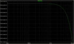
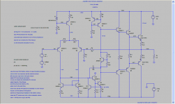
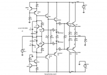
Reading about Bakerclamps in your book I implemented some in the joined circuit. Are these well placed?
For information : OPS is still not implemented nor is the bias circuit.
Off-course, anyone is free to comment on the clamps, but on the whole circuit too !!!
For now simulation shows 1.6ppm THD20 at full swing - not loaded (only vas & ips, no ops!).
Cheers,
Olivier
Hi Bob,
Reading about Bakerclamps in your book I implemented some in the joined circuit. Are these well placed?
For information : OPS is still not implemented nor is the bias circuit.
Off-course, anyone is free to comment on the clamps, but on the whole circuit too !!!
For now simulation shows 1.6ppm THD20 at full swing - not loaded (only vas & ips, no ops!).
Cheers,
Olivier
Attachments
fft profiles
Hi Bob,
abusing of your attention ... and apropos of this insightful discussion about NFB.
What do you think about these FFT's profiles? It is a 62W (8 OHM) Class AB amp, Gain=21, output quiescent current of 500ma, 70° PM, 165V/usec slew ... note the exponential monotonic harmonic fade out. The FFT's are at 30W output power pix 1: 100KHZ, pix2: 20KHZ and pix3: 2KHZ . It is the final design of the prototype I plan to build.
Cheers
Arturo
Last edited:
- Home
- Amplifiers
- Solid State
- Bob Cordell's Power amplifier book