Well, it turns out Qco is sometimes present and sometimes not, depending on luck and what kind of simulation you are using. Definitely seems like a bug. I got it working on Greenamp. Qco=1n had a moderate effect.
In this simulation it has no effect. It is an Ft chart generator, go to view->error log->Rclick->plot.
In this simulation it has no effect. It is an Ft chart generator, go to view->error log->Rclick->plot.
Attachments
Hey Bob, is your new book going to be available in Kindle format from Amazon? I prefer to read it on my computer so I can easily switch back and forth to LTSpice to check things as I read.
I see it's already available for pre-purchase, but I don't see an electronic format.
Thanks, gabo
I see it's already available for pre-purchase, but I don't see an electronic format.
Thanks, gabo
To the best of my knowledge it will not be available in Kindle. Less than 10% of the first edition sold were Kindle, and there was a lot of pirating due to its availability in Kindle (Kindle DRM is broke and there is SW out there to make a perfect PDF from a Kindle file).
Best,
Bob
Best,
Bob
I downloaded the book of Bob Cordell to my cell.. I have been reading it a little and it seems to me the book Is great!..Nice acknowledgment. I would like to build one of His amplifiers but I don't know which one, one with 100 or 200 watts class AB to share it with my friends. Thank you.
Any idea when the paperback copy will be released ? Why this great delay after ordering it ?
The web site tells me that they will inform me by email !
Hi Ashok,
Thanks for your interest in my second edition. Amazon shows it as available May 31. It is not unusual for publishers to offer new books for preorder before they are printed. My first edition was available for preorder 6-8 weeks before publication. I think they do it partly for publicity and maybe to get an early feel for the demand. It may also have some influence on the size of the print run and perhaps production priorities (among multiple books scheduled for publication in the same time frame, who gets access to the printing presses first). Just speculation on my part.
I'm reviewing the proofs as we speak
") .
.Cheers,
Bob
Hi Bob.
I was going over the details of setting bias current in you book. Pages 47 to 50 and had a question.
You mention that the gain of the output stage changes as the output impedance changes especially when you go from Zo small signal when the output resistance is in parallel to Zo large signal.
My question is when exactly does this change from Zo small signal to Zo large signal happen.
I would like to try and model this as you have done in you book. I have attached my spreadsheet which I have started.
Attachments
Last edited:
Hi Stuart,
The way I usually look at this issue is with a wingspread simulation, as carried out on page 399 of the LTspice chapter. The phenomenon is shown fairly well in the wingspread plot on page 187. If you look at the wingspread for the over-biased condition, it is fairly easy to see how the small-signal output stage gain condition transitions to the large-signal gain situation. When looking at a wingspread of an optimally-biased output stage, the transition is a little less obvious due to the wiggles in the output stage gain in the crossover region. To some extent, the explanation of the static crossover distortion phenomenon is an heuristic argument.
One thing to bear in mind is that ohmic emitter resistance in the power transistor, and base resistance divided by beta, effectively appear as part of the external emitter resistor. This makes the emitter resistor look like a larger value, insofar as meeting the Oliver condition goes. The end result is that in reality the optimum voltage across the external emitter resistor is usually less than 26 mV. In evaluating this, it is also important to recognize that base stopper resistance makes an ohmic contribution divided by beta just as does the internal RB of the transistor. A 2.5-ohm base stopper with a transistor beta of 50 will contribute 0.05 ohm to the ohmic resistance seen looking into the emitter all by itself. And this assumes that the base stopper resistor is driven by a true voltage source, which it is not.
Cheers,
Bob
Speaking of Barney Oliver, here's the relevant section of the paper he wrote. Not somebody else's interpretation or summary. The original. You may have to click on the image one or two times to see it full size and undistorted.
Look for the expression "13 to 26 millivolts".
Oliver does not say "26 millivolts". He says "13 to 26 millivolts".
~
Look for the expression "13 to 26 millivolts".
Oliver does not say "26 millivolts". He says "13 to 26 millivolts".
~
True, but in this context he appears to be saying that the optimum voltage across the external emitter resistor may be less than 26 mV as a result of changes in kT/q as a function of junction temperature, not as a result of an ohmic component of transistor emitter resistance as seen looking into the emitter of the power transistor.
A brilliant paper, no matter how you look at it.
He even envisioned the advent of the ThermalTrak transistors!
Cheers,
Bob
A brilliant paper, no matter how you look at it.
He even envisioned the advent of the ThermalTrak transistors!
Cheers,
Bob
No, Vt doesn't change that much from 300-400k. I think "between 1/2Go[=1/2Vt] and 1/Go[=Vt]" refers to a different mechanism.
The reason the range extends below 26mV is because while 26mV results in a better average distortion when operating above the crossover region, it does this by creating a gain dip at the crossover point, thus creating the W shape in the wingspread chart.
This means that although large-signal distortion has been decreased, small-signal distortion at the crossover point has been increased.
When you reduce the emitter degeneration voltage, the W turns into a U, and at about 13mV (or thereabouts) you get a plateau at the bottom of the U which is very linear. This is good for signals below the crossover threshold, bad for signals above it. So if you want a linear class A stage using a complimentary EF, this is an often overlooked way of attaining it. Barney's observation of the thermal feasibility of low degeneration voltage is a significant concern.
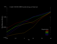
You might remember this graph I created years ago using your simulation models with a voltage driven EF, which shows the interesting effect of lower degeneration voltages. The chart shows a null at 10mV for low output. There may have been a few mV extra across the base stoppers and internal base resistance.
The reason the range extends below 26mV is because while 26mV results in a better average distortion when operating above the crossover region, it does this by creating a gain dip at the crossover point, thus creating the W shape in the wingspread chart.
This means that although large-signal distortion has been decreased, small-signal distortion at the crossover point has been increased.
When you reduce the emitter degeneration voltage, the W turns into a U, and at about 13mV (or thereabouts) you get a plateau at the bottom of the U which is very linear. This is good for signals below the crossover threshold, bad for signals above it. So if you want a linear class A stage using a complimentary EF, this is an often overlooked way of attaining it. Barney's observation of the thermal feasibility of low degeneration voltage is a significant concern.
You might remember this graph I created years ago using your simulation models with a voltage driven EF, which shows the interesting effect of lower degeneration voltages. The chart shows a null at 10mV for low output. There may have been a few mV extra across the base stoppers and internal base resistance.
Attachments
Last edited:
Oops, I really messed up that first paragraph. Ic/2Gm=1/2Vt and Ic/Gm=Vt. Oliver seems to mean something a bit different by Io. But it seems clear to me he is not referring to Vt changing with temperature when he gives 13-26mV as the valid range.
You can download the paper here, although it is a bit blurry:
Barney Oliver: Crossover Distortion in Class B Audio Amplifiers
You can download the paper here, although it is a bit blurry:
Barney Oliver: Crossover Distortion in Class B Audio Amplifiers
Oops, I really messed up that first paragraph. Ic/2Gm=1/2Vt and Ic/Gm=Vt. Oliver seems to mean something a bit different by Io. But it seems clear to me he is not referring to Vt changing with temperature when he gives 13-26mV as the valid range.
You can download the paper here, although it is a bit blurry:
Barney Oliver: Crossover Distortion in Class B Audio Amplifiers
Yeah, I didn't take that away from what he wrote either, and when you look between 300K and 400K on >10^16 doping of silicon, the number of intrinsic carriers is too small to modulate the threshold voltage.
Obviously Vbe/Ib vs temp is a different kettle of fish.
*With large devices where we have far less body effect on gating.
I get distortion minimized from about 60% of the Oliver voltage - so ~18 mV - up to about 30 mV so it’s quite flat in my case. This can be useful in a big amp with parallel output pairs where you may want to save on standing power consumption. I have a 240 watt design (6 parallel pairs) that I run at 18 mV per side (36 mV a pair with 0.33 Ohm emitter degen resistors). On a smaller 100 watt unit, I am running at the full 26 mV - seems to sound a bit sweeter, but I may well be imagining that bit.
- Home
- Amplifiers
- Solid State
- Bob Cordell's Power amplifier book