Good point about pre-amp build-out resistance.
Some designs may use values more like 50 ohms or 75 ohms,
In other cases, a designer might try to build out to a "standard" impedance, like 600 ohms.
Cheers,
Bob
So, might be a good thing to do during design - if CMR is important - to see how sensitive one's design is to CMR and diff ips z unbalance.
An input buffer would minimize change due to Z unbal on line. It will add some small cost but maybe add distortion also.
The higher you can make the Zo of the diff ips tail current source the better. but really high Zo over wide freq isn't so easy.
-RM
Last edited:
So, might be a good thing to do during design - if CMR is important - to see how sensitive one's design is to CMR and diff ips z unbalance.
An input buffer would minimize change due to Z unbal on line. It will add some small cost but maybe add distortion also.
The higher you can make the Zo of the diff ips tail current source the better. but really high Zo over wide freq isn't so easy.
-RM
This is my CFA version with balanced input. Simulation showed no significant THD increase with a buffer at inverting input. I have yet to try it in real amp.
Damir
Attachments
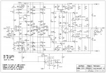
This is my CFA version with balanced input. Simulation showed no significant THD increase with a buffer at inverting input. I have yet to try it in real amp.
Damir
Looks a bit... complicated. I would urge you to build and measure it at the first opportunity.
Herein lies the mechanism. In order for that correction to take place, the base drive of the slave transistor must have a distorted version of the VAS collector signal on it. Any SPICE simulation will show that, even given the fairly simplistic modeling of Early effect by SPICE. When that bias line (the base of the VAS slave current source transistor) is also used by the tail current source, the tail current will be modulated by that correction signal, propagating that distortion into the input current via the finite beta of the input stage transistors. This is obviously an unwanted interaction between the VAS and the IPS. One additional cheap transistor and one resistor solves the whole problem by implementing two independent feedback current sources for the tail current and VAS pull-up current. This is an example of KISS - don't try to be cute by sharing a bias line between the IPS and the VAS. Simple as that.
At the risk of repeating myself excessively, the downside of trying to save a penny or two on biasing components is fully expounded in the 6th edition, even if not every diagram complies with separate biasing.
The point I made earlier today was that there is no detectable CM distortion in the input stage so long as you have a reasonable closed-loop gain, independently of the biasing details. This is a matter of experiment and measurement, not just simulation.
I hear you may have a second edition coming out. I hope you will not think me discourteous if I ask you if there any actual measurements in it?
Are-you the Douglas Self that answered to a member of this forum, telling-you that you cannot put CFAs under silence in a technical book about amplifiers.: "Yes I can !" ?Looks a bit... complicated. I would urge you to build and measure it at the first opportunity.
The asymetrical version of Dadod's amp has been build and measured by at least two different members, with amazing low distortion (40V, 0.002% 20kHz ?), high slew-rate results.
A bit complicated, indeed.
Last edited:
I am interested by the topology of common mode loops (using Q1-Q4 on the schematics below) in amplifiers having a differential VAS as they have been proposed by :
Bob Cordell in his HEC-MOSFET amp
Samuel Groner ( page #48 http://www.nanovolt.ch/resources/power_amplifiers/pdf/audio_power_amp_design_comments.pdf )
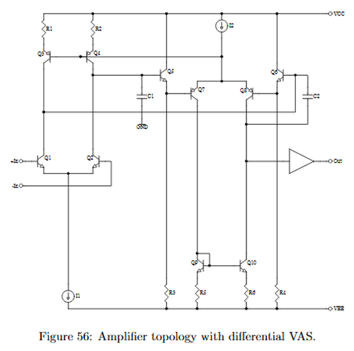
Could these schemes do some good against common mode distortion and how could they compare with floating cascodes in the input pair?
Bob Cordell in his HEC-MOSFET amp
Samuel Groner ( page #48 http://www.nanovolt.ch/resources/power_amplifiers/pdf/audio_power_amp_design_comments.pdf )
Could these schemes do some good against common mode distortion and how could they compare with floating cascodes in the input pair?
Attachments
So, might be a good thing to do during design - if CMR is important - to see how sensitive one's design is to CMR and diff ips z unbalance.
An input buffer would minimize change due to Z unbal on line. It will add some small cost but maybe add distortion also.
The higher you can make the Zo of the diff ips tail current source the better. but really high Zo over wide freq isn't so easy.
-RM
The THAT InGenious differential input IC does a great job at this.
Yes, very high impedance in the tail current source is desirable. If one wants to go really crazy, one solution is a cascoded feedback current source. One can do the cascode with either a BJT or a JFET. Many other approaches to achieving very high output impedance also work well. Capacitance can be gotten down to 1-3pF. Since there is usually headroom to burn in a power amp tail current source, I will often stick a resistor in series with the collector of the current source to keep the impedance fairly high and resistive even at really high frequencies. This might help EMI immunity. Depending on the tail current and the available headroom, this resistance might be between 2k and 10k.
Cheers,
Bob
At the risk of repeating myself excessively, the downside of trying to save a penny or two on biasing components is fully expounded in the 6th edition, even if not every diagram complies with separate biasing.
The point I made earlier today was that there is no detectable CM distortion in the input stage so long as you have a reasonable closed-loop gain, independently of the biasing details. This is a matter of experiment and measurement, not just simulation.
I hear you may have a second edition coming out. I hope you will not think me discourteous if I ask you if there any actual measurements in it?
That is indeed a discourteous and snide remark. There were a ton of measurements in the first edition. I do not use an AP, so virtually all of my measured data was plotted using graphic software. Anyone who looks at what was new in your 6th edition will see that much of that new material was inspired by and along the same lines as, issues that I brought up my first edition - and without proper attribution.
I do not apologize for heavy use of SPICE simulation as a teaching tool in my book. It is a marvelous tool to provide insight. Measurements are important as well both for showing achieved performance and for unraveling the cause of some circuit behaviors whose origins are elusive. However, measurements can be imprecise and subject to interpretation. I believe that there are a number of occasions where you made measurements and speculated wrongly about what was going on. In cases like that, the use of SPICE simulation to augment your measurement results and sanity-check your conclusions would have been helpful. I am also glad that I was able to introduce SPICE in the context of audio amplifier design to a large population with the book. I think that SPICE modeling was also important to cover, especially given the very poor manufacturers' models that are out there.
Speaking of measurements, countless hours were spent carefully measuring a large number of real transistors to come up with the Cordell models. Those kinds of measurements are far more difficult than hooking up an AP to an amplifier and flipping a switch. Please also bear in mind that almost 35 years ago I built and MEASURED a MOSFET power amplifier with error correction and reported distortion levels less than 0.001% at 20kHz up to full power. I'm not sure that, to this day, you have achieved that level of performance in any of your designs. You might want to review that paper; it is on my web site.
Yes, I have a second edition coming out, and it will be published by Focal/Taylor & Francis, the same publishers as yours.
Your point earlier about there being little or no CM in the input stage is not relevant to the issue I have pointed out about your sharing of current source bias lines introducing distorted feedback into the tail current source. Regardless of your motivation for sharing that bias line, be it saving a few pennies or trying to look clever, it is a dumb idea.
Bob
Hum ... if it is not, it really looks like...discourteous.I hope you will not think me discourteous if I ask you if there any actual measurements in it?
The THAT InGenious differential input IC does a great job at this.
It's exceedingly good. Whilst it does add measurable distortion the levels are so low as to be not worth worrying about other that spec drag racing IMO. And whilst there are lower noise ways of doing a balanced input it's advantages when dealing with unknown source balance make it almost a no brainer for $3 in a domestic setting.
I do wonder why more people who worry about getting to sub 10ppm distortion measurements don't take balanced lines at least to the power amp more seriously. It's a very marmite* thing.
* for those who have not come across yeast extract based spread, you either love it or hate it, no middle ground. AKA vegimite in australia
Negitive Feedback
Hi All,
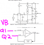
I just wanted to double check that the error signal that is use in the amplifier from the differential pair can be measured and taken directly from the base of Q1 and Q2. So the error factor is VB(Q2) - VB(Q1)? This number multiplied by the Aol = Vout
Hi All,
I just wanted to double check that the error signal that is use in the amplifier from the differential pair can be measured and taken directly from the base of Q1 and Q2. So the error factor is VB(Q2) - VB(Q1)? This number multiplied by the Aol = Vout
Attachments
Looks a bit... complicated. I would urge you to build and measure it at the first opportunity.
It is a little more complex - a bit. however --yesterday I measured with 2 Ohm load, 10KHz, .007% THD at 700W !
At <200W into any load or freq is well under .001%. Stable as a rock. 400 V/usec. Very quiet.
THx-RNMarsh
Last edited:
It is a little more complex - a bit. however --yesterday I measured with 2 Ohm load, 10KHz, .007% THD at 700W !
I thought you had built the SE version?
It is a little more complex - a bit. however --yesterday I measured with 2 Ohm load, 10KHz, .007% THD at 700W !
At <200W into any load or freq is well under .001%. Stable as a rock. 400 V/usec. Very quiet.
THx-RNMarsh
Dear Richard,
we have some major difference in our measurements of Damirs 200W CFA. I have measured this slew rate:
- 10kHz square rising edge (slew: 70V in 250ns ~ 280V/µs)
- 10kHz square falling edge (slew: 70V in 375ns ~ 200V/µs)
200W into any load and frequency also different: 200W MOSFET CFA amp
My measurements differ from yours significant. It looks like your test sample has a different - more aggressive - compensation or is different in using other components?
IMHO: the amplifier has very good values - I do not want to make Damir's amplifier look bad in any way! I just want to know why we measure such different values...
We could continue this discussion in Damir's thread or start a new one.
BR, Toni
Hi All,
I just wanted to double check that the error signal that is use in the amplifier from the differential pair can be measured and taken directly from the base of Q1 and Q2. So the error factor is VB(Q2) - VB(Q1)? This number multiplied by the Aol = Vout
Yes, this is true, up until the unity-loop-gain frequency (i.e., the frequency at which the loop came is equal to 1), beyond which it gets more complicated.
- Home
- Amplifiers
- Solid State
- Bob Cordell's Power amplifier book