Harry, you seem to have avoided the "stupid ray" or what ever it is that affects people so they write abuse rather than actually look at any data.
Thank you. I try hard to keep ego out of it. I am just interested in learning the truth. I accept that I don't know everything (far from it), that I sometimes make mistakes, and that there are plenty of people out there cleverer than me. I liked a post you made in another thread:
To dispel a falsehood is not to kick a man but to free him from error.
Search only for the truth and do not hold on to beliefs from pride.
This is called "Free yourself of attachment to illusion".
It is the path of wisdom.
I liked a post you made in another thread:
Thank you. I should explain the context for the pseudo-Chinese style parody was to amuse Mr Lee, but I do actually believe it.
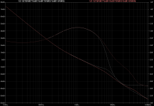
But what about this phase response? I think I understand it now but still interested to read comments.
Best wishes
David
Attachments
Last edited:
I must have missed it
I reposted it above
... a non-minimum phase system is one with singularities in the RHP, be they zeros or poles.
That makes a TIS a non-minimum phase system.
RHP poles don't make very satisfactory amplifiers.
")
I am somewhat surprised just how much non-minimum phase.
Best wishes
David
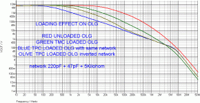
For a fair comparison, one has to compare apples and apples, which requires that the compensator component values be made identical in both cases.
Using the same network will indeed yield almost the same results
distorsion wise in the relevant band but at very high frequency
the VAS/TIS gain will be seriously shaped by the loading effect
of the capacitor that goes to its output , hence , the VAS/TIS high
frequency response with TPC wont be exactly the same as with TMC
wich doesnt suffer this loading to some extent , we could even assume
that connecting the bigger capacitor to the output node with TPC
will add some inherent shunt compensation , moreover with low
values of the grounding resistance.
OTA means Operational Transconductance Amplifier.
The two first stages of most power amplifiers are Miller compensated OTA .
Completly wrong I am afraid. The first stage of most amplifiers is a transadmittance amplifier (viz. voltage to current amplifier), while the second stage is a transimpedance amplifier (viz. current to voltage amplifier).
Therefore the first two stages of most amplifiers taken together constitute a voltage amplifier and not an OTA.
In this case we would have a Miller OTA showing all pass property around the zero. There are of course well known ways to avoid this trap like a resistor in serie to make the zero negative or making the capacitor path unilateral ( Ahuja) . Then the positive zero disapears.
Simple SPICE simulation should demonstrate that the RHP zero does not give an all-pass characteristic to the transimpedance stage (TIS).
Secondly, as I have pointed out previously, the RHP zero is of no consequence if you use a BJT-based transimpedance stage, as it will typically reside well beyond forward path unity gain frequency. This may not be the case with a MOSFET TIS because a MOSFET's transconductance is more than an order of magnitude smaller than that of a BJT. This is why Miller compensation about a MOSFET TIS requires a resistor in series with the compensation capacitor.
Please remain educated in your reaction. I was asked to explain and I did it...I accept a demonstration and not agressive assertions close to be insulting.
Please don't be silly! Where in my post, which I have reproduced below, have I made "agressive assertions close to be insulting" (sic)?
First, in what context are you using the acronym "OTA"? I.e. what does "OTA" stand for?
Secondly I have read Lundberg, Gray and Mayer, Solomon and Roberge from cover to cover. Nowhere in those works is it suggested, particularly with a BJT TIS, that the second pole (or first non-dominant pole) precedes the RHP zero.
As I have indicated previously, the RHP zero resides well beyond unity gain for a BJT TIS and is at a higher frequency than the first two dominant poles.
Therefore, at no point do you have a flat frequency response before unity gain due to the RHP zero. Moreover, due to the presence of non-dominant poles after the onset of the RHP zero it is highly improbable that you'll have a flat all-pass frequency response even after the RHP zero takes effect.
Last edited:
For a fair comparison, one has to compare apples and apples, which requires that the compensator component values be made identical in both cases.
That's unreasonable Mike and not at all required for an apples vs apples comparison.
I'd agree to an equal number of components, but if resistor in TPC is 10k and in TMC is 8k, that is still a perfectly reasonable apples-to-apples.
jan
Using the same network will indeed yield almost the same results
distorsion wise in the relevant band but at very high frequency
the VAS/TIS gain will be seriously shaped by the loading effect
of the capacitor that goes to its output...
This need not be the case. If loading of the TPC network on the TIS's output is an issue, simply connect the larger of the two capacitors to the input of the TIS. Problem solved.
I disagree. Profoundly.
The only fair comparison is one that guarantees the same loop gain about the output stage with TPC and TMC, and, simultaneously, gives virtually the same unity loop gain frequency and stability margins.
The above can only be guaranteed by using the same compensator component values for TPC and TMC as I have previously demonstrated.
Hi Mike,
There are many combinations of C1, C2 and R1 that satisfy both of your criteria to a quite adequate degree of accuracy. I suspect that you have not done enough simulations with different ratios of C2 to C1 where the ULGF has been held the same and the amount of loop gain about the output stage at 20kHz has been held the same.
For this reason, it is not necessary to make all fair comparisons between TPC and TMC with identical values of C1, R1 and C2.
Cheers,
Bob
That's unreasonable Mike and not at all required for an apples vs apples comparison.
I'd agree to an equal number of components, but if resistor in TPC is 10k and in TMC is 8k, that is still a perfectly reasonable apples-to-apples.
jan
Hi Jan; good to hear from you.
Actually, the resistor in both compensation schemes (TPC and "TMC") establishes the location of the LHP zero that is required to restore a single pole roll-off (from an initial double-pole roll-off).
Now, if the loop transmission of the whole amplifier with TPC is to be the same as the loop transmission about the second stage and the output stage with "TMC", and, additionally, if the two schemes are to give virtually the same unity loop gain frequency and stability margins for the loop enclosing the second stage and the output stage with "TMC", and the whole amplifier with TPC, then the location of the zero must be the same. This is why the resitor in TPC must be identical to the resistor in "TMC" for an apples and apples comparison.
I demonstrated this by simulation a while ago in this thread.
I suspect that you have not done enough simulations with different ratios of C2 to C1 where the ULGF has been held the same and the amount of loop gain about the output stage at 20kHz has been held the same.
Hi Bob,
Sometime ago in this thread, I requested that you produce by simulation or otherwise "...different ratios of C2 to C1 where the ULGF has been held the same and the amount of loop gain about the output stage at 20kHz has been held the same..." I did not receive a response.
I hold that to maintain the same loop gain across the audio band with the same location of the zero and the same unity loop gain frequency and stability margins, the component values for both TPC and "TMC" have to be the same, as I have previously demonstrated.
Now, if I am wrong I would very grateful for a demonstration of this.
Last edited:
Completly wrong I am afraid. The first stage of most amplifiers is a transadmittance amplifier (viz. voltage to current amplifier), while the second stage is a transimpedance amplifier (viz. current to voltage amplifier).
Whether you call it a transadmittance or transimpedance stage depends on what exactly?
V * Ym = I
V / Zm = I
Both equations apply to the input stage. So what's the difference?
Bob and many others appear to prefer the measure of Gm for transistors. I prefer to use Rm instead. Gm is arguably more useful for common-collector stages and Rm more useful for emitter-followers. In both cases it is nothing but a matter of convenience and random preferences.
And are we following the distinction between transistor stages and transistor configurations? The TIS could be seen as a V-I converter that's been converted to an I-V stage by input and output resistors. But what if you consider the TIS input resistor part of the input stage? Then the TIS is a current amplifier and the IPS a voltage amplifier. Egads!
I think we are hopelessly overconfident in our veiled subjective preferences.
 Read Solomon below:
Last edited:
This need not be the case. If loading of the TPC network on the TIS's output is an issue, simply connect the larger of the two capacitors to the input of the TIS. Problem solved.
Not solved but slightly displaced.
But why not checking all thoses loading effect with simulators.?
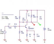
Attachments
Are you being deliberately obtuse? You do realise that this is just a semantic argument? That Bob used the term "excess phase" in not strictly-speaking the "correct" or "usual" way? Indeed, that is why I put it in quotes when I tried to help out several posts ago.
Bob was using the term "excess phase" to refer to the phase shift at ULGF contributed by the high-frequency poles. If you can make this "excess phase" smaller, by using faster devices, you can move the ULGF to a higher frequency whilst maintaining the same phase margin. That is all.
Very competent people use the term , see MichelKiwanuka link
in the post above , it s just unfortunate that it becomes a problem
by there , i hope that such semantic discussions are put to rest
since this bring nothing in the table other that useless confusions.
Thanks for this, JPV.OTA means Operational Transconductance Amplifier.
The two first stages of most power amplifiers are Miller compensated OTA .
I was referencing these authors to start from a common understanding of the open loop Miller OTA transfer function and its well known approximations. If you take the generic transfer function as explained in let say Lundberg and if you simplify for widely separated poles and large Cmiller you can get:
To summarize (for large Cmiller and gm2):
gain bandwith : gm1/2piCmiller
freq of zero : gm2/2pCmiller
non dominant pole : gm2/2piCload this non dominant pole is created in the OTA, it is not a non dominant pole coming from the class AB buffer poles although the input capacitance of this buffer is included in Cload.
If Cmiller is >> Cload the zero is at lower frequency than the non dominant pole. From a phase point of view, a positive zero acts as a pole. To be able to stabilize such a circuit, this singularity should be at least 3 times the GBW frequency to have enough phase margin ( rule of thumb), this can be achieved with gm2>3 gm1
In this case we would have a Miller OTA showing all pass property around the zero. There are of course well known ways to avoid this trap like a resistor in serie to make the zero negative or making the capacitor path unilateral ( Ahuja) . Then the positive zero disapears .
If these tricks are not used, the OTA stage is non minimum phase because it has a positive zero and the amp with feedback is still non minimum phase because if I recall well a basic property of control theory: the zeros of the open loop transfer function are the zeros of the closed loop function.
Using Blacks formula: F(s)= G(s)/1+G(s) H(s) if G(s) = N(s)/D(s) then
F(s) = N(s)/(D(s) + N(s)H(s))
It is the best accurate explanation of plain Miller I've seen. Your clarity approaches that of Great Guru Baxandall. I shall now pre10 2 unerstan it to bolster my facade as a (pseudo) guru and use it confound the truly pseudo pontificating that abounds.
______________________
Mike, you have demonstrated loadsa stuff. Alas ALL your demos (at least the SPICE sims) seem to have appalling THD & stability. IMHO, none of them would be stable with 'real life' loads.michaelkiwanuka said:I demonstrated this by simulation a while ago in this thread.
Few of us are concerned with the difference between pig sh*t and cow sh*t. Apples & oranges would be better compared in something with some semblance to a 'good' amp.
Bode plots on sims of wonky amps look testicle but it would be good to show improvements of your beloved TPC against TMC on something with 'good' performance. 'Real life' would be nice but you seem to spurn any such evidence.
In the meantime, SPICE THD & stability with different loads will do for a start.
______________________
Waly, if I read you correctly, your 'reliable measurements' are solely about Loop Gain and Phase Margin. Can you confirm this?Waly said:I was able to confirm through reliable measurements in our university lab that TMC and TPC are exactly equivalent. This should be understood in the sense that given a TMC compensated amp, there is a TPC compensation that provides exactly the same loop gain and phase margin.
...
What others measured on power amplifiers, I have no idea, but I am not under the impression this forum is anywhere focused on reliable lab measurements.
I'm rather saddened that you discount the efforts of those who at least attempt 'real life' measurements. I for one am far more interested in these than dubious pontificating by various pseudo prophets.
While I'm happy to generate pages of semantic and pedantic diarrhea, I'm under no illusion that these even approach the practical usefulness of my 'Definitive Dissertation on VAS vs TIS'
As you are a Budding True Guru, I counsel you not to indulge in Excess Phase less you join the ranks of pedantic pseudo prophets.
To summarize (for large Cmiller and gm2):
gain bandwith : gm1/2piCmiller
Ok
freq of zero : gm2/2pCmiller
Ok
non dominant pole : gm2/2piCload this non dominant pole is created in the OTA, it is not a non dominant pole coming from the class AB buffer poles although the input capacitance of this buffer is included in Cload.
Don't understand "non-dominant pole created in the OTA". Who is Cload other than the next stage input cap?
If Cmiller is >> Cload the zero is at lower frequency than the non dominant pole.
Why would one make Cmiller >> Cload? I would think this would be highly unusual in audio amplifiers.
From a phase point of view, a positive zero acts as a pole.
Ok
To be able to stabilize such a circuit, this singularity should be at least 3 times the GBW frequency to have enough phase margin ( rule of thumb), this can be achieved with gm2>3 gm1
Ok, this condition is practically always fulfilled in audio amplifiers.
In this case we would have a Miller OTA showing all pass property around the zero. There are of course well known ways to avoid this trap like a resistor in serie to make the zero negative or making the capacitor path unilateral ( Ahuja). Then the positive zero disapears.
There are essentially three methods to compensate RHP zeroes: as you said, a resistor in series with the Miller cap, a voltage buffer [1], or a current buffer [2]. See also http://www.ece.ucdavis.edu/~hurst/papers/MillerComp,CAS1.pdf and http://dr.ntu.edu.sg/bitstream/handle/10220/4680/Gain-Enhanced%20Feedforward%20Path%20Compensation%20Technique%20for%20Pole-Zero%20Cancellation%20at%20Heavy%20Capacitive%20Loads.pdf?sequence=1
If these tricks are not used, the OTA stage is non minimum phase because it has a positive zero and the amp with feedback is still non minimum phase because if I recall well a basic property of control theory: the zeros of the open loop transfer function are the zeros of the closed loop function.
If all these are happening beyond the UGF (which seem to be always the case in audio amplifiers), then what would be the relevance? In fact, you don't even need an OTA to get the same results; a simple common emitter circuit will reveal the same effect, see below. As I mentioned before, each and every common emitter (or source, or cathode) gain stage has a RHP zero, because of the Cob (or the equivalent for tubes, jfets, mosfets, etc...).
Outside audio, there are indeed cases (like in CMOS opamps, where due to the low transconductance of the devices the RHP zero can indeed occur around or before the UGF) where taking care of the RHP zero really matters. Otherwise, in my opinion, unless one chooses a pathological audio design only to make a point, the RHP zero issue in audio amplifiers can be safely ignored.
[1] P. E. Allen and D. R. Holberg, CMOS Analog Circuit Design. London, U.K.: Oxford Univ. Press, 1987.
[2] B. K. Ahuja, “An improved frequency compensation technique for CMOS operational amplifiers,” IEEE J. Solid-State Circuits, vol. SSC-18, pp. 629–633, Dec. 1983.
[2] B. K. Ahuja, “An improved frequency compensation technique for CMOS operational amplifiers,” IEEE J. Solid-State Circuits, vol. SSC-18, pp. 629–633, Dec. 1983.
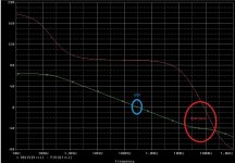
Attachments
Last edited:
Err.rh! This is sorta the usual case with plain Miller compensated amps .. unless you subscribe to Mike's propensity to slug the VAS output with evil capacitance to cure all ills, Re or Im.Why would one make Cmiller >> Cload? I would think this would be highly unusual in audio amplifiers.
Some designers are more '>>' eg Self than others eg Cordell. But doesn't alter JPV's excellent analysis except for da pedants.
The rest of your stuff is OK and agrees with JPV once you get past da semantic/pedantic niggles. [deleted : 2 pgs on >> vs > vs nearly =]
_____________
Can you confirm your 'reliable measurements' are solely about Loop Gain and Phase Margin?I was able to confirm through reliable measurements in our university lab that TMC and TPC are exactly equivalent. This should be understood in the sense that given a TMC compensated amp, there is a TPC compensation that provides exactly the same loop gain and phase margin.
Did you do any THD measurements?
Last edited:
Can you confirm your 'reliable measurements' are solely about Loop Gain and Phase Margin?
Did you do any THD measurements?
Yes and no.
Don't understand "non-dominant pole created in the OTA". Who is Cload other than the next stage input cap?
As I've pointed out, it's not an "OTA"; it's a voltage amplifier.
- Home
- Amplifiers
- Solid State
- Bob Cordell's Power amplifier book