No.But as you say, since the late 80's we have much better devices available. IME, a 50W @8R amp can get away with simple fuses in the PSU leads.
 All amps. need SOA protection of the single slope or double slope variety at least.
Thank you Bob,
Yes, that is the stuff that would be of interest to myself and most likely others. How to add cap filtering to basic two transistor (or led biased) CCS's. Seems like just adding a cap across the v ref part of it would help some, but I rarely see anyone at all do that. Wondering if there is a reason they do not.
I have downloaded LTspice and hope to figure out how to use it at some point. Got a few things figured out, but a long way to go before I trust anything as results.
Regards,
Greg
Hi Greg,
Let me make sure I was clear. Most references for current sources require a bias current, such as the current that must flow through the LED or the Zener that acts as the reference. Same for the current that is made to flow into the reference transistor in the 2-transistor feedback current source. This current is often supplied by a resistor to ground when the current source is from the supply rail. This resistor should be split, and the junction of the two parts should be bypassed to the rail, filtering noise from that biasing current.
For a current source based on a reference like an LED, the LED can also be bypassed to remove its noise, but, as jcx pointed out, it is more effective to bypass the reference voltage produced by the LED after that voltage has passed through a series resistance (it is more effective to bypass a higher-impedance node with a capacitor than a low-impedance node).
Bypassing nodes within the 2-transistor feedback current source is usually not productive because that tends to defeat the action of that feedback loop.
Cheers,
Bob
Wouldn't that transfer PS garbage into the circuit ? For eg, as in my screenie. If a Cap is placed across the top Res in a "Virtual" Ground application, it will do exacly that !
Or did you mean placing a Cap from the CCS to Ground ? Wouldn't that cause issues too though ?
Hi Zero D,
I think I was too ambiguous in my original reply to Dan. See my subsequent reply about using a shunt capacitor to filter the biasing current fed to the current source. That capacitor forms an R-C lowpass filter that is referenced to the voltage node to which the current source is connected. In the case of a simple pull-down LED-transistor current source, that capacitor would be tied to the node where the LED cathode is connected.
Sorry for any confusion.
Cheers,
Bob
Hi Bob,
In your book you suggest Darlington VAS(page 60, fig. 3.7) as an evolution. There is a situation in case of overdrive that transistor acting as emitter follower(Q12) could be forced to conduct to much current and burns taking some other transistor with it and the output goes to one side polarity. It can damage the loudspeaker too, I had it happened to me. A simple solution(discussed in this forum sometime) is to add a resistor between Q12 collector and the ground, 1kohm is a good value. I came to that solution long time ago after almost destroyed loudspeaker. D. Self missed that protection resistor too.
BR Damir
Hi Bob,
In your book you suggest Darlington VAS(page 60, fig. 3.7) as an evolution. There is a situation in case of overdrive that transistor acting as emitter follower(Q12) could be forced to conduct to much current and burns taking some other transistor with it and the output goes to one side polarity. It can damage the loudspeaker too, I had it happened to me. A simple solution(discussed in this forum sometime) is to add a resistor between Q12 collector and the ground, 1kohm is a good value. I came to that solution long time ago after almost destroyed loudspeaker. D. Self missed that protection resistor too.
BR Damir
Hi dadod,
Thanks for pointing this out, but I think Edmond addressed the issue unless I am mistaken. First of all, the resistor in series with the Darlington (EF) transitor's collector up to ground is a reasonable way to protect against this, and bypassing the collector of the darlington to ground can probably overcome any high-frequency implications. I suppose one could also pick the resistance value to allow some deliberate voltage drop in the collector circuit to decrease dissipation in the Darlington transistor. However, even with the resistor, the current pulled by the VAS transistor could be quite high and cause asymmetrical slew behavior.
The better solution is the feedback current limiting transistor that Edmond mentions. In principal, the current limit enforced by that transistor can be set to twice the current of the VAS load current source in the classic single-ended VAS amplifier arrangement to achieve at least similar overload behavior in each direction.
Let me know if you think I've missed something here.
Cheers,
Bob
Hi Bob,
Edmond is right, I may case there was no the feedback current limiting transistor, but the collector resistor did not introduced more phase shift in my simulations and I would keep collector resistor just in case.
BR Damir
Originally Posted by Bob Cordell
That capacitor forms an R-C lowpass filter that is referenced to the voltage node to which the current source is connected
Ahh, well that's more like it
Thanks
Hi Bob,
Edmond is right, I may case there was no the feedback current limiting transistor, but the collector resistor did not introduced more phase shift in my simulations and I would keep collector resistor just in case.
BR Damir
Yes, I also usually add a collector resistor to the EF transistor of VAS. It does not effect small signal analysis very much.
I don't like put a current limit resister to the Emitter of VAS. I believe it will reduce the open loop gain.
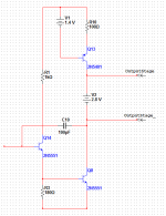
And I want to introduce another way, using saturated current source to do the current limiting of EF transistor. Please see the second picture.
I use this way in my last amplifier.
Attachments
I don't like put a current limit resister to the Emitter of VAS. I believe it will reduce the open loop gain.
No; that resistor has no effect on the gain of the second stage.
You can also provide effective VAS/TIS current limiting by cascoding the amplifer transistor(s) and then inserting a resistor between the amplifier transistor collector and the cascode emitter.
This has little or no effect on practical amplifier performance and works very well.
This has little or no effect on practical amplifier performance and works very well.
Hi Bob,
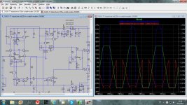
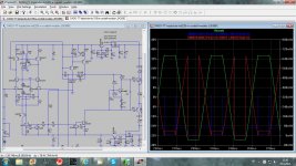
Here is overload VAS simulations with and without collector resistor in emitter follower enhaced VAS.
It looks that this resistor is still needed even with VAS protection transistor.
What do you think?
BR Damir
Here is overload VAS simulations with and without collector resistor in emitter follower enhaced VAS.
It looks that this resistor is still needed even with VAS protection transistor.
What do you think?
BR Damir
Attachments
You can also provide effective VAS/TIS current limiting by cascoding the amplifer transistor(s) and then inserting a resistor between the amplifier transistor collector and the cascode emitter.
This has little or no effect on practical amplifier performance and works very well.
Actually, during the clipping, the output current of VAS won't be large. The output stage won't taken any more current than the normal situation. The current is limited by the current source of the VAS. We don't need to limit the current for whole VAS. The problem is too much current on base pin of the 2nd transistor. It is over driven by the EF transistor in Enhanced VAS.
Last edited:
Actually, during the clipping, the output current of VAS won't be large. The output stage won't taken any more current than the normal situation. The current is limited by the current source of the VAS. We don't need to limit the current for whole VAS. The problem is too much current on base pin of the 2nd transistor. It is over driven by the EF transistor in Enhanced VAS.
You perhaps missed the context. If you could look at the schematic on page 60 of Cordell's book which is the circuit in question here, when it is driven into clip and the amp therefore goes open loop, Q12 can souce quite a big deal of current into emitter juction of Q4 and burn it up if Q13 wasn't there. The current souce load of Q4 would be irrelevant when this had ever happend, as it would only limit the collector current.
Last edited:
You perhaps missed the context. If you could look at the schematic on page 60 of Cordell's book which is the circuit in question here, when it is driven into clip and the amp therefore goes open loop, Q12 can souce quite a big deal of current into emitter juction of Q4 and burn it up if Q13 wasn't there. The current souce load of Q4 would be irrelevant when this had ever happend, as it would only limit the collector current.
The problem is not the Ic of Q4. The problem is Q12 push too much current on the BE junction of Q4. The Ic of Q4 never goes up during clipping.
In that case, limiting Ic of Q12 is more important and more straightforward to this issue.
Last edited:
Hi Bob,
Here is overload VAS simulations with and without collector resistor in emitter follower enhaced VAS.
It looks that this resistor is still needed even with VAS protection transistor.
What do you think?
BR Damir
Hi dadod,
I'm having a little bit of trouble interpreting the plots. Looks like the right scale is in mW of power dissipation, rather than ma of current. Can you explain which color is a plot of what?
Also, just to be sure, can you state what the VAS current source load is set to and also what the VAS current limiter is set to?
Thanks,
Bob
The problem is not the Ic of Q4. The problem is Q12 push too much current on the BE junction of Q4. The Ic of Q4 never goes up during clipping.
In that case, limiting Ic of Q12 is more important and more straightforward to this issue.
Ah, I came to realize you were going against the idea of a resistor between the collector and the emitter in a cascoded VAS setup. Now I'm on the same page with you.
Ah, I came to realize you were going against the idea of a resistor between the collector and the emitter in a cascoded VAS setup. Now I'm on the same page with you.
Yes, you were right. The resistor between the collector and the emitter in a cascoded VAS, it won't work.
Hi dadod,
I'm having a little bit of trouble interpreting the plots. Looks like the right scale is in mW of power dissipation, rather than ma of current. Can you explain which color is a plot of what?
Also, just to be sure, can you state what the VAS current source load is set to and also what the VAS current limiter is set to?
Thanks,
Bob
Hi Bob,
First picture no protection resistor, second picture 1kohm protection resistor.
VAS standing current 9.3mA, protection set to four time more.
Yellow plot- output voltage
Blue plot - power disipation on Q15(EF) right scale
Red - power dissipation on Q12(VAS)
I hope this will help.
BR Damir
- Home
- Amplifiers
- Solid State
- Bob Cordell's Power amplifier book