mikeks said:...loop transmission at 20KHz is typically 25dB~30dB, while DPC can be persuaded to deliver ~60dB at the same frequency.
Mike,
I just tried a real quick sim of this comp network and saw some distortion improvements. I made C2 and C3 each equal to 2C (don't have any idea if that's right or not BTW - it was just a quick guess). It looks promising. Puts the output stage in the local VAS feedback loop at low freqs but gets it out of the way at high freqs So it prevents the local loop instability that output-stage-inclusive compensation has (Cherry's "world's cheapest oscillator" trick
") ).
).Attachments
mikeks said:Have you examined major loop transmission at 20KHz for before/after improvements?
Yes. It was actually about 4 dB less with the modified configuration above than the original (standard two-pole comp). Unity loop gain frequency was about the same. I think more improvements are possible. I want to understand this better - not just component values, but maybe the topology itself could be improved. Ideally, I'd like the major loop transmission to be unchanged, and have the output stage get out of the minor loop at maybe 1 MHz or so (not sure).
The unity loop gain freq of my VAS is scary high, so there's absolutely no way the Cherry-style output stage-inclusive comp could ever be stable.
mikeks said:This accomplishes nothing as far as linearity is concerned: loop transmission at 20KHz is typically 25dB~30dB, while DPC can be persuaded to deliver ~60dB at the same frequency.
Hi Mike
First, do me a favor and revert to a terminology we all can understand, so loop GAIN, not loop transmission.
Second, what do you mean by ‘DPC’? Never heard of it, neither do google or dogpile.
And please, don’t forget that you have already caused much of a trouble on this forum by using your own a terminology.
As far as the transfer function of the global feedback loop concerned, indeed, it’s unaltered and it should be that way. So, what’s your point? Do you suggest that because of this, the thd figures are unaltered too?
Anyhow, my sims show a thd reduction of about 15dB.
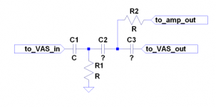
And for those who are intending to run a sim, please use a VAS, as depicted below. Don’t use a Darlington, by tying the collectors of Q2 and Q3 together. The Early effect and Cob modulation of Q2 spoils the whole thing.
Attachments
Estuart refering to a compensation scheme encompassing the output stage and needing a beta enhancement transistor in the VAS stage makes me to think of the Cherry's NDFL amplifier. The NDFL amplifier described in ETI May 1983 contains a Rush pair (a common collector PNP loading the input stage followed by a common base NPN ahead of a main voltage gain PNP).
mikeks said:Enclosing a power BJT output stage provokes local instability even with a series resistor.
Hi Mike,
Apparently, you doesn’t understand much of my compensation. At least Tim__X does. At one point you are right: Enclosing a power BJT output stage provokes local instability, that is, at fairly high frequencies, 10…20MHz. However, at frequencies that high, my circuit behaves just like a traditional Miller compensated amp and is rock stable. Maybe you should have a closer look at my diagram (it’s clear enough I think) and discover that I don’t use just a single resistor to prevent instabilities, rather an RC network. As a result, below 230kHz, determined by the time constant R1*(C1+C2), my arrangement behaves just like Cherry’s thing, above that frequency, it slowly revert to a conventional and safe scheme, as I said before.
Regards.
forr said:DPC : Double Pole Compensation ?
Thanks forr!
Normaly, it's called TWO pole compensation, hence the confusion.
(just google it)
Hi Edmond,
Sometimes NFB arrangements like the one you show can reduce THD at higher audio frequencies but increase 'first cycle' or transient distortion and actually impair output stage control of a dynamic loudspeaker.
Thus reactively tuned THD optimisation can degrade reproduction.
Cheers .......... Graham.
lumanauw said:Hi, Estuart,Your schematic in post #497, how to determine the value of C1-C2-R1? Is there any paper/article about it?
Hi lumanauw,
The equivalent series capacitance of C1 and C2 should be equal to the original Cdom. The are no strict rules for choosing C2 and R1, but the impedance of network C2 & R1 should chosen such that it is not too much loaded by C1. So, if C2 is 5 to 10 times C1, it’s OK. Regarding R1, see my previous post.
Cheers,
Hi, Estuart,
Thanks for the explenation
Your compensation scheme reminds me of a work of Lars Clausen.
It is different, it is about taking feedback point. Feedback point is taken parrarel between VAS/C6=1nf and output/R24=1k. Then this parrarel point is taken to differential.
Thanks for the explenation
Your compensation scheme reminds me of a work of Lars Clausen.
It is different, it is about taking feedback point. Feedback point is taken parrarel between VAS/C6=1nf and output/R24=1k. Then this parrarel point is taken to differential.
Attachments
mikeks said:...while DPC can be persuaded to deliver ~60dB at the same frequency.
Hi Mike,
Now I see what you mean: TWO pole compensation(TPC), rather off topic, hence the confusion.
Indeed, linearity can be improved by increasing the bandwidth of the global feedback loop. By means of TPC however, is the worst thing you can do. I repeat myself, have look at post 466 and 467. The phase margin at 10…20kHz is terrible low. This does not imply that the system is unstable, but it causes a considerable amount of overshoot. So forget this miserable thingy.
Linearity can also be improved by increasing the loop bandwidth around the O/P stage (that’s what I’m doing), leaving the global feedback loop and step response unaffected.
Convince yourself by running a sim (I suppose you do have a decent simulator, otherwise end of discussion), one with R1 (in my diagram) tied to ground and one with R1 tied to the output. THD should be the same, step response differs.
BTW, use a VAS as shown on post 505, nothing else!
Regards,
estuart said:
Hi Mike,
. This does not imply that the system is unstable, but it causes a considerable amount of overshoot. So forget this miserable thingy.
I’ve been spicing TPC to see how good it is in comparison to other methods for a <1ppm THD-20 500W+ amplifier design I’ve almost finalised. I though it was great at first, examining the resultant slew rate. Then I did a bode plot into a reactive load. Looked like one of Evil Knievel’s motorcycle ramps.........
Cheers,
Glen
EDIT: Oops. Terminology confusion. Not TPC, although I've seen people call it TPC. Not the TPC you are talking about, I think.
Arrggh.lumanauw said:Hi, Estuart,
Your compensation scheme reminds me of a work of Lars Clausen.
Hi lumanauw,
Funny. Indeed, based on same principle, except that feedback is led to a different point. Probably doesn’t work with BJTs in the O/P stage, but with MOSFETs it’s OK.
Interested in an other example (which I simulated, but not build)?
Do I have papers on this subject? No, nothing, sorry.
Cheers,
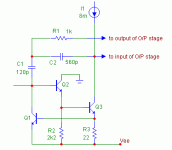
Hi Graham,Graham Maynard said:Using a resistor from output to Darlington VAS base can also help to reduce output stage crossover distortion and improve NFB response by flattening the open loop bandwidth.
Using an equal value resistor from other half of mirror to ground prevents start-up thump and preserves differential input balance.
This is a Sim demo cct only.
I note the use of a relatively low Iq value.
The improvement in output stage distortion reduction will probably be more evident when the stage is under-biased.
If the Iq is re-set to 70mA, will the benefits of the revised NFB be as marked?
Will the results be changed at all when a higher IQ is set?
Edmond, let's cut to the chase: what is major (global) loop transmission (gain) with your set up compared with ordinary Miller compensation?
http://www.diyaudio.com/forums/showthread.php?postid=1160075#post1160075
http://www.diyaudio.com/forums/showthread.php?postid=1160075#post1160075
estuart said:
Exactly, that’s the crux. Chapeaux!
See below for this simple but valuable trick.
Note: It doesn’t work without a preceding beta enhancement transistor in the VAS stage. Probably, that’s why D. Self misunderstood the potential of this subtle modification.
Cheers,
Who originally came up with this form of compensation?
It seems to be a fairly nice and inexpensive trick. As described by others, it looks basically like Miller compensation taken from the output of the power stage, but then bypassed (transitioned) to use the more stable output of the VAS itself by C2 and R1 at a frequency on the order of 250 kHz. I think that this topology might benefit from connecting C2 to an emitter-follower (fast) buffered output of the VAS. This would isolate the VAS from currents flowing in R1. This emitter follower could just be the first guy in the output triple.
Double pole compensation has value, but it needs to be used carefully. There are not too many truly free lunches. However, careful selection of its component values allows one to exercise a tradeoff between minimum phase margin and amount of loop gain enhancement it delivers at 20 kHz.
A more generalized approach is to seek a loop gain rolloff on the order of a constant 9 dB/octave, which gives a phase margin on the order of about 45 degrees. This is just a compromize between the conservative 6 dB/octave and the deadly 12 dB/octave. Indeed, double pole compensation ("T" compensation as it was called at Bell Labs in the 1970's where we integrated it into op amps) can be thought of as just one form of approximation to 9 dB/octave compensation.
Bob
Hi, Estuart,
Please submit them
I have 1 question. What happens if I don't use buffer before VAS (omitting Q2 in your graph, the input differential pair directly feds base of Q3)?
Off courseInterested in an other example (which I simulated, but not build)?
Please submit them
I have 1 question. What happens if I don't use buffer before VAS (omitting Q2 in your graph, the input differential pair directly feds base of Q3)?
Bob Cordell said:It seems to be a fairly nice and inexpensive trick. As described by others, it looks basically like Miller compensation taken from the output of the power stage, but then bypassed (transitioned) to use the more stable output of the VAS itself by C2 and R1 at a frequency on the order of 250 kHz. I think that this topology might benefit from connecting C2 to an emitter-follower (fast) buffered output of the VAS. This would isolate the VAS from currents flowing in R1. This emitter follower could just be the first guy in the output triple.
Bob
Edmond's arrangement can only be said to constitute an "improvement" if the later is expressed as an increase in loop gain in the audio band without compromising stability.
- Home
- Amplifiers
- Solid State
- Bob Cordell Interview: Negative Feedback