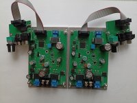
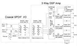
I have assembled such a light version board that has sparked interest among people for using it in their projects.
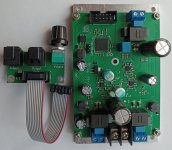
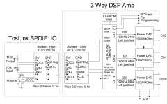
For this board to work when creating your project, the ADAU1452 must be synchronized with the DAC.
The quickest and easiest way is to use my file as a base.
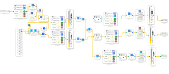
I have attached the file to this message, which contains all the necessary settings for the board. In this file, you can add blocks that you need, but not all blocks from this project can be deleted. Later in the thread, I will describe what and why is done in this file, so that you can confidently create projects on this board for your needs.


For this board to work when creating your project, the ADAU1452 must be synchronized with the DAC.
The quickest and easiest way is to use my file as a base.

I have attached the file to this message, which contains all the necessary settings for the board. In this file, you can add blocks that you need, but not all blocks from this project can be deleted. Later in the thread, I will describe what and why is done in this file, so that you can confidently create projects on this board for your needs.
Attachments
Last edited:
On this board, the PWM DAC is implemented using the FPGA capability. The DAC receives a data stream from the ADAU via the I2S bus, the DAC acts as a master of the I2S bus and requests a data stream from the ADAU with a sampling frequency of 192 kHz, 24 bits, left justified.
In order for the DAC to receive the correct data, the output port I2S0 and I2S1 of the ADAU 1452 must be configured as a slave with clocking from CLK domaine 0.

Usually the project frequency is different from 192 kHz, so to create a data stream on the I2S output port with a frequency of 192 kHz you need to use UpSampling, in my example the project frequency is 48 kHz, and to get a data stream of 192 kHz I need to multiply the project frequency by 4. If you create a project with a frequency of 96 kHz, then you need to set UpSampling to 2, and if you have a project at 192 kHz, then UpSampling needs to be removed from the project.
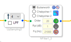
For UpSampling to work correctly, its output must pass through a low-pass filter (LPF), the UpSampling block itself has its own LPF, but its cutoff frequency starts at 15 kHz, if you need to have a more even frequency response in the channel at frequencies above 15 kHz, then you need to disable the internal LPF in UpSampling, and apply an additional low-pass filter with a cutoff frequency of 21 kHz, then the frequency response will be more even at 15-20 kHz. What I did in the shown project is stere plus one. If the frequency response rolloff above 15 kHz is acceptable, then you can apply an internal low-pass filter in UpSampling, which I do in the low-frequency channel for ch16.
For the DAC to work correctly, the ADAU must output a data stream with a frequency of 192 kHz to its I2S output, you need to monitor this, if you remove UpSampling and apply a data stream with a frequency of 48 kHz to the I2S port, nothing will break, the DAC will just start producing a lot of extra harmonics .
Using an external potentiometer and auxiliary ADC to adjust the volume.
In this basic project, I implemented volume control using this scheme.
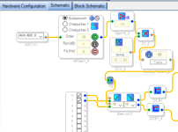
The voltage values obtained from the ADC are fed to a low-pass filter, which eliminates all the noise that penetrates from the outside world into the useful signal; if you remove this low-pass filter, then all the noise that comes to the input of the ADC will interact with the useful signal, this filter is very important.
After the filter, a scheme for converting the bit depth of a number is implemented and then a table is applied that specifies the curvature of the volume control. If the curvature of the volume control does not suit you, then by changing the values in the table you can customize it for yourself.
You can also change the signal processing algorithm from the ADC using other modules, but it is very important to use a low-pass filter after the ADC, otherwise noise will creep into the signal.
If external signal volume control is not needed, then this module can be excluded from the project.
In this basic project, I implemented volume control using this scheme.

The voltage values obtained from the ADC are fed to a low-pass filter, which eliminates all the noise that penetrates from the outside world into the useful signal; if you remove this low-pass filter, then all the noise that comes to the input of the ADC will interact with the useful signal, this filter is very important.
After the filter, a scheme for converting the bit depth of a number is implemented and then a table is applied that specifies the curvature of the volume control. If the curvature of the volume control does not suit you, then by changing the values in the table you can customize it for yourself.
You can also change the signal processing algorithm from the ADC using other modules, but it is very important to use a low-pass filter after the ADC, otherwise noise will creep into the signal.
If external signal volume control is not needed, then this module can be excluded from the project.
DC Blocking (DCB) Module
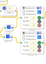
Sometimes programs using the spdif output fail and a constant component appears at the spdif output; the DCB module prevents the appearance of a constant voltage at the output of the ADAU in the event of failures in the spdif source.
Also, the DAC itself has protection against the constant component of the signal at its output; the DAC monitors the output of each channel and checks for the presence of constant voltage.
When a constant voltage appears at the output, the DAC turns off the power PWM chip, after a second of delay the DAC turns on the PWM chip, and if a constant voltage is again present at the DAC output, the chip turns off after ten cycles and the LED begins to blink. Only the channel on which there is constant voltage is turned off.
Therefore, if you somehow apply a constant voltage to the input of the DAC, it will go into protection after 10 seconds. If a constant voltage is present at the output for ten cycles, the DAC turns off this channel until the board is completely turned off.
This board does not require additional devices to protect speakers from DC voltage or protection from clicks when turning the power on and off. This board has no clicks when turning the power on and off, and there is also control and protection against the presence of constant voltage at the DAC output.
However, when creating your project, sometimes conditions are created that lead to overload of the DAC input, and or loud clicks at the DAC output. Therefore, I recommend that while debugging your project, apply a reduced voltage to the board with a current stabilization function, for example 12V 1A, thereby you will reduce the number of unexpected events.
100W per channel is actually a lot, and if for one reason or another a 100W click appears at the output of the DAC, then it will hit the ears very well.
After DC Blocking, I installed a high-pass filter with a cutoff frequency of 10 Hz so that the speakers would not receive frequencies below 10 Hz, which may appear for one reason or another in the original signal, this high-pass filter is not critical and can be removed if you do not see the need for it.
Matching the levels of the input signal and the output signal of the ADAU with the DAC.
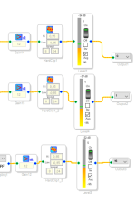
The DAC is configured in such a way that it produces a maximum amplitude voltage of 28V at its output when the ADAU outputs 0dB to the DAC input.
I usually adjust the gain in the ADAU in such a way that with an input signal of 0dB(Fs), the output of the ADAU receives 0dB, which I control using level indicators. I adjust the gain by changing the values in the signal amplification block. Now the gain is configured in such a way that with an input signal of 0dB(Fs), the ADAU will output 0dB.
If you change the gain to a higher level and output more than 0 dB to the input of the DAC, then the DAC will be overloaded at the input and the protection in it will start to work, and at the same time the output of the PWM amplifier implemented on TAS, which also has protection against overload of its output, will be overloaded, as a result Various unpredictable voltage changes will begin at the DAC output, as the protections will begin to compete with each other.
The DAC overload in this board always has a different character and it is best not to overload the DAC input, but to cut the signal inside the ADAU at 95% using the HardClip hardware module. This module also protects the DAC input from unintentional errors when debugging your project, for example, when using an automatic equalizer, you can accidentally amplify the signal by more than 0 dB and thereby overload the DAC input at a certain frequency.
Sometimes, in order to improve the level of dynamics in a multi-way speaker, you need to reduce the channel gain by 3 dB or more, this can be done by reducing the value of the amplification modules, but increasing the gain more than 0 dB and disabling HardClip is highly not recommended.
It is important to monitor the level of the maximum signal that the ADAU produces on the DAC.
It is convenient to check the maximum gain setting in the channels with the load turned off at the board output using the level indicators in the Sigma Studio environment.
Automatic equalizer.
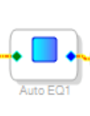
A very convenient module when there is a need to obtain the desired frequency response at the output of the speaker based on the real frequency response that was obtained using a microphone, as an example, using the free REW program you can obtain the frequency response and save it in a format that Sigma Studio can read.
Having a text file of the frequency response with the help of Avto EQ it is very easy to obtain an arbitrary frequency response at the output of the DAC.
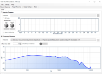
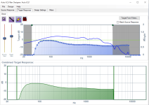
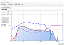
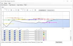
Later I will show how I used the capabilities of the automatic equalizer of Sigma Studio when correcting the frequency response in my three-way digital active speakers with FIR band division.

A very convenient module when there is a need to obtain the desired frequency response at the output of the speaker based on the real frequency response that was obtained using a microphone, as an example, using the free REW program you can obtain the frequency response and save it in a format that Sigma Studio can read.
Having a text file of the frequency response with the help of Avto EQ it is very easy to obtain an arbitrary frequency response at the output of the DAC.


Later I will show how I used the capabilities of the automatic equalizer of Sigma Studio when correcting the frequency response in my three-way digital active speakers with FIR band division.
Today I checked another board and discovered my mistake in my basic Sigma Studio project.
For the low-frequency channel (Ch16), I sum the left and right channels, and this is essentially an increase in the signal by 3 dB, and I did not reduce the gain in Ch16. As a result, at maximum volume at the ADAU input, an overflow of the DAC input should appear at the Ch16 output, but since I used the HardClip module this does not happen, it protects the DAC from overflow. A very useful HardClip module for this board.
For the low-frequency channel (Ch16), I sum the left and right channels, and this is essentially an increase in the signal by 3 dB, and I did not reduce the gain in Ch16. As a result, at maximum volume at the ADAU input, an overflow of the DAC input should appear at the Ch16 output, but since I used the HardClip module this does not happen, it protects the DAC from overflow. A very useful HardClip module for this board.
Using the board as a stereo amplifier with a channel for a subwoofer does not fully reveal the potential of the adau1452 and the speakers.
To get better sound from speakers using this board, it is best to make an active three-way speaker.
In the folder that I attached earlier there is a project file as one of the possible options for using a board with an FIR crossover.
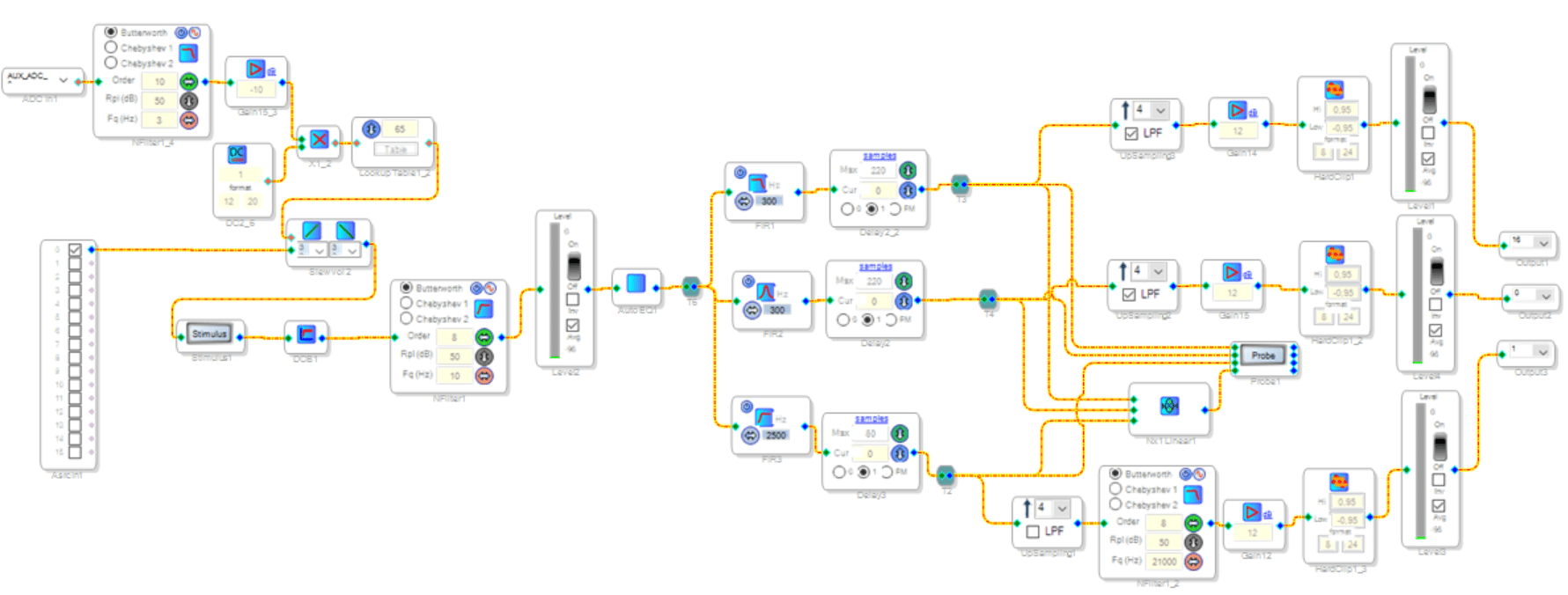
In this project I used library FIR filters to split the signal into three bands.
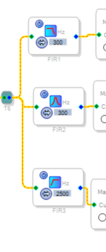
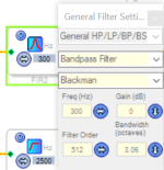
As can be seen from the filter settings, the first filter from the top is a low-pass filter with a cut-off frequency of 300 Hz, then there is a band-pass filter with a pass-through frequency of 300-2500 Hz and then a high-pass filter with a cut-off frequency of 2500 Hz, all filters are set to order 512.
To control the correct settings of filters, Sigma Studio has a convenient tool - a probe.
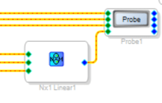
The probe shows what comes to its input after pressing the stimulus button. It is very convenient for them to control changes in the frequency response of a signal by a project, within the project itself.
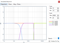
By changing the filter settings to suit your needs, you can immediately see how this affects the final frequency response, and the frequency response in each band.
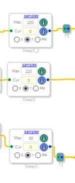
After the filters there is a delay line; it is necessary to coordinate the acoustic centers of the speakers with each other. I adjust the delays using step response.
I have already described the remaining blocks earlier and they should not raise any questions.
To get better sound from speakers using this board, it is best to make an active three-way speaker.
In the folder that I attached earlier there is a project file as one of the possible options for using a board with an FIR crossover.
In this project I used library FIR filters to split the signal into three bands.

As can be seen from the filter settings, the first filter from the top is a low-pass filter with a cut-off frequency of 300 Hz, then there is a band-pass filter with a pass-through frequency of 300-2500 Hz and then a high-pass filter with a cut-off frequency of 2500 Hz, all filters are set to order 512.

To control the correct settings of filters, Sigma Studio has a convenient tool - a probe.

The probe shows what comes to its input after pressing the stimulus button. It is very convenient for them to control changes in the frequency response of a signal by a project, within the project itself.

By changing the filter settings to suit your needs, you can immediately see how this affects the final frequency response, and the frequency response in each band.
After the filters there is a delay line; it is necessary to coordinate the acoustic centers of the speakers with each other. I adjust the delays using step response.

I have already described the remaining blocks earlier and they should not raise any questions.
I use signal merger to sum signals. It automatically reduces the inputs so they won't overflow. I typically use it for summing channels for a subwoofer output.Today I checked another board and discovered my mistake in my basic Sigma Studio project.
For the low-frequency channel (Ch16), I sum the left and right channels, and this is essentially an increase in the signal by 3 dB, and I did not reduce the gain in Ch16. As a result, at maximum volume at the ADAU input, an overflow of the DAC input should appear at the Ch16 output, but since I used the HardClip module this does not happen, it protects the DAC from overflow. A very useful HardClip module for this board.
https://wiki.analog.com/resources/t...lbox/mixerssplitters/signalmerger?force_rev=1
Very nice! How are you sending I2S to DAC - how does DAC request I2S data stream?On this board, the PWM DAC is implemented using the FPGA capability. The DAC receives a data stream from the ADAU via the I2S bus, the DAC acts as a master of the I2S bus and requests a data stream from the ADAU with a sampling frequency of 192 kHz, 24 bits, left justified.
In order for the DAC to receive the correct data, the output port I2S0 and I2S1 of the ADAU 1452 must be configured as a slave with clocking from CLK domaine 0.
As I understand it, you are asking how the board accepts I2S?Very nice! How are you sending I2S to DAC - how does DAC request I2S data stream?
If this is the case, then on the board there is an ADAU I2S input port which is connected to pins, the input port itself is configured in SigmaStudio under the necessary conditions, it can be either a master or a slave, with different variations, all of which are supported by the ADAU1452. A complete list of all possible settings for the I2S input port can be found in the description of the ADAU1452 chip or simply go to the I2S input settings in SigmaStudio. Since the adau1452 has fairly good asynchronous sample rate converters (ASRC), there is no need for frequency synchronization between the source and I2S receiver.
When the adau operates in the slave, the stream given from the external I2S source must be passed through the ASRC ADAU1452. In my basic project, adau is configured to receive an I2S stream via ASRC1, and ASRC0 is configured to receive SPDIF.
I understand that you have a DSP and some kind of DAC with an I2S input and you cannot get sound at the DAC output?
I can’t answer what your problem is. Much depends on the capabilities of the DAC you want to use. I will only say that if your DAC needs a Master clock, then the ADAU has a special clock frequency pin, which can be configured in Sigma Studio to generate a frequency.
I can’t answer what your problem is. Much depends on the capabilities of the DAC you want to use. I will only say that if your DAC needs a Master clock, then the ADAU has a special clock frequency pin, which can be configured in Sigma Studio to generate a frequency.
I don't want to hijack this thread, all the details are here: https://www.diyaudio.com/community/threads/awdsp8x-4way-stereo-dsp2dac-board-with-adau1452.410839
I found measurement results in my archives when I was playing with setting up three-way speakers on FIR filters.
Below in the picture, the red frequency response is before correction, the black frequency response is after correction, and the most interesting thing further is the step response of this whole undertaking.
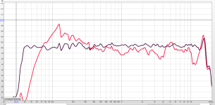
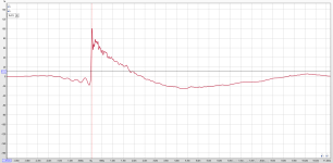
I’ll say right away that listening to speakers with such an frequency response is very problematic because the entire sound is exposed, the slightest flaws in the mixing of the music can be heard, later I took a different approach, it allowed me to find some kind of compromise between musicality and sound detail.
But what is so interesting about these pictures? They show the capabilities of FIR filters in ADAU1452.
Below in the picture, the red frequency response is before correction, the black frequency response is after correction, and the most interesting thing further is the step response of this whole undertaking.


I’ll say right away that listening to speakers with such an frequency response is very problematic because the entire sound is exposed, the slightest flaws in the mixing of the music can be heard, later I took a different approach, it allowed me to find some kind of compromise between musicality and sound detail.
But what is so interesting about these pictures? They show the capabilities of FIR filters in ADAU1452.
I think it’s worth moving these messages here, not everyone followed these boards in the other thread.
The schematic indicates that the board implements an I2C port specifically for programming the ADAU1452.
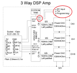
The DSP has been programmed with a basic project firmware to verify the board's parameters.
I also provide this project in SigmaStudio format in the first post of this thread in the attached file. The project contains all the DSP settings needed to synchronize the DSP with the board. Without these settings, creating a new project would be quite problematic, as it requires knowledge of some settings, such as the board's clock speed, etc.
Please note that to achieve an average power of 100W per channel, the power supply must deliver a peak current of 18.75A. This is a lot, and not every power supply can withstand such current. However, this is not always necessary. If the board is used in active speakers, the main power will be distributed to only one channel, reducing the peak power consumption of the power supply by three times.
Yes.Can the DSP can be programmed via SigmaStudio using the 3 terminal I2C connector and a standard USBi programmer?
The schematic indicates that the board implements an I2C port specifically for programming the ADAU1452.

The DSP has been programmed with a basic project firmware to verify the board's parameters.
I also provide this project in SigmaStudio format in the first post of this thread in the attached file. The project contains all the DSP settings needed to synchronize the DSP with the board. Without these settings, creating a new project would be quite problematic, as it requires knowledge of some settings, such as the board's clock speed, etc.
When supplying the board with a 32V power voltage, an additional heatsink is required. The total power consumption of the entire board at 32V power supply ranges from 9W to 11W, depending on the temperature of the heatsink. By default, the board is mounted on a plate heatsink with sufficient effective area, which is only enough when the board is powered up to 20V. Beyond 20V, an additional heatsink is necessary. If there's no actual need for 100W per channel, it's optimal to apply a lower power supply voltage to reduce the board's power consumption.Are heatsinks recommended/required on the 3 chips on the bottom of the board?
I use switching regulated power supplies, including flyback converters or push-pull power supply. The board isn't overly demanding in terms of power source quality since it has local voltage regulators. The main thing is to avoid using extremely poor power sources that generate significant noise and can't sustain the required peak output current.What did you use for a power supply?
Please note that to achieve an average power of 100W per channel, the power supply must deliver a peak current of 18.75A. This is a lot, and not every power supply can withstand such current. However, this is not always necessary. If the board is used in active speakers, the main power will be distributed to only one channel, reducing the peak power consumption of the power supply by three times.
The board is already mounted on a plate heatsink. This plate heatsink has holes at the corners, allowing it to be attached to a larger heatsink if desired. You can remove the board from the basic plate heatsink, and attach it to another larger plate heatsink. To increase the distance between the power chips and the plate heatsink aluminum heat conductors, 3mm in height, are used to achieve this. Thus, using heat conductors, the board is lifted 3.5mm away from the heatsink, ensuring that surface mount components have the necessary air gap from the heatsink.Regarding the heatsink: do those 3 chips stand higher than the the other components so a single plate heatsink could be used to cover all three? Or is a separate, smaller heatsink required for each chip?
- Home
- Source & Line
- Digital Line Level
- Board 3-Way PWM DAC with DSP ADAU1452 - 100W per channel
