Hi audiofan,
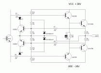
So you want to include a protection cct - but not limit the current in T12. You need the emitter resistor of 0.3V/Iq (how lazy am I), and two diodes or a BJT to clamp base drive.
Your protection cct all but turns on with no output current at full opposite swing which will modulate Vas gain, so best to slug it heavily - 10uF.
Still the old Vas and 100pF.... hohum.
Cheers,
Greg
with my experience ,
-two pole compensate network has a lower distiontion than single pole if we only consider low harmonics ,example 2nd ,3rd
-but with higher harmonics ,two pole is worse than single pole
distorion only become a considerable thing if input signal frequency is higher than 7khz,8khz
the distortion is only a few hundred uV with low signal frequency
if input signal is 8kz ,2nd will be 16khz and 3rd will be 24khz . We can't hear the 24khz sound
Hi Thanh,
Very good -
...if input signal is 8kz ,2nd will be 16khz and 3rd will be 24khz . We can't hear the 24khz...
But 24KHz can intermodulate with 23KHz and blast you out your rear window at 1KHz, into the lap of a bunch of Australian football neanderthals!!! You wouldn't want that now.
Cheerrs,
Greg
Very good -
...if input signal is 8kz ,2nd will be 16khz and 3rd will be 24khz . We can't hear the 24khz...
But 24KHz can intermodulate with 23KHz and blast you out your rear window at 1KHz, into the lap of a bunch of Australian football neanderthals!!! You wouldn't want that now.
Cheerrs,
Greg
i made a modification to protection circuit and now protection will not cause the same problem
at saturation I= 6.8 amp
at 20 volts Vce I= 5 amp
at 35 volts Vce I= 3.6 amp
at 50 volts Vce I=2.15 amp
at 70 volts Vce I= 2 amp
expect that it will cure a part of the problem
at saturation I= 6.8 amp
at 20 volts Vce I= 5 amp
at 35 volts Vce I= 3.6 amp
at 50 volts Vce I=2.15 amp
at 70 volts Vce I= 2 amp
expect that it will cure a part of the problem
Attachments
Hi,
that's 140Watts when driving a reactive load. Not many output transistors can take that when derated firstly for voltage and secondly for case temperature.
Your A1986 can take 0.95A at 70 volts and with a case temperature about 10Cdeg above your heatsink temperature, this will reduce to about 0.5A to 0.8A.
Even at 35V you will need to take account of both derating factors to check that your protection locus does actually do it's job. By the way I suggest you allow for peak current = Vpk/Rload when Vce = Vrail i.e. for 8ohm load 4.75A at Vce=38V and Ppk=180Watts. To be able to drive any severe 8ohm speaker load you will need 2 pairs of your 150W output transistors and this will also be able to drive a mild mannered 4ohm speaker load.
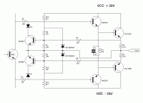
Andrew I read your note , and you were right I was asking for too much on output transistors. I read carefully the transistors specs an come back with a new optimisation of protection circuit, so for:
Vce = 0 volts Ie =5.9 amp
Vce = 35 volts Ie = 2.5 amp
Vce = 70 volts Ie = 0.75 amp
This is more realistic for transistor operation.
I also read your note on how much current the amp should deliver, and if I use your figure the amp will be able to deliver 50 VA in an 8 ohms fully reactive load ( capacitor or inductor bank ) that is certenly ideal condition but need a very though amp.
With the value I expect to use the amp will deliver 50 VA in an 8 ohms load at 45 dege of phase shift. I expect this to be acceptable since I use a pair of speaker with a fair cross over with no resonnant circuit, or if resonnant damped with a resistor. I should not have deep impedance dip or heavy phase shift.
thanks for the valuable info.
Attachments
Hi Audiofan,
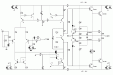
T13 increases your current gain around the VAS just as Self. OK.
C22 has a very low impedance at high audio frequencies and above and will severely load the LTP. It will seriously interfere with sound quality. Try reducing this to below 22pF and preferably do without it all together and use other compensation techniques to stabilise the amp. This HF feedback around the VAS is, in my opinion, why many reviewers criticise the sound of Self's amp designs. I suspect that the current mirror load on the LTP also has some detrimental effect on sound quality, although there are many reputable designs that use one or other and sometimes both of these design features.
Is the decoupling cap C21 connected to the correct reference?
If I understand correctly input signal ( voltage ) of T13 & T12 is beetwen Base of T13 and node commun to R67 & R22, so if we dont want to inject noise supply of collector must be filtered with VEE as reference.It is not possible to do in another way since R70 is betwen ground and T13 collector, if I connect C21 to ground it will be in parallel wit R70 and will inject more noise. I used the same analysis as used fo C1 in upper side for current source. By the way many thanks for your help.
audiofan said:If I understand correctly input signal ( voltage ) of T13 & T12 is beetwen Base of T13 and node commun to R67 & R22, so if we dont want to inject noise supply of collector must be filtered with VEE as reference.It is not possible to do in another way since R70 is betwen ground and T13 collector, if I connect C21 to ground it will be in parallel wit R70 and will inject more noise. I used the same analysis as used fo C1 in upper side for current source. By the way many thanks for your help.
Hi Audiofan,
VEE is NOT what we want as a reference here, R22 is forming a low pass filter together with C11||C9 and is absolutely correct in such topology.
Our Amp.guru Greg, among others too, have treated this issue quite well in his thread.
Cheers Michael
Hi,
I see in my prevous post that I read earlier audiofan's post as VEE ishould be the reference, but he didn't say that directly, I read his post too quickly.
However, I think C 21 is correct as the signal at this side is actually V-gain stage rail supply referenced (R67 says).
But it's a tiny issue comparing to looking at "the other side" of the VAS tansistor, here the signal get's ground referenced, so the 100 pF C22 is a worser problem than compared to T13's intrinsinc Miller cap.
And those current mirrors, don't know what to say... it's a high impedance output stage and it almost take over the role of being the culprit from the VAS.
Cheers Michael
I did go to that "killer amp thread " bu my english is not fluent so for me it would take a few weeks 24/7 to perfectly understand but I read it and it used very different configuration ( far away of RCA and self ) but they are working aroud power supply rejection power supply noise and rating and many others points.
I ad R70 & C21 to get a better power supply rejection , R22 & C9 & C11 are a standard power supply rejection circuit often seen at many places. In my point of view to current loop around T13 in my configuration is completed with C21 ( C21, T13, R71) and it dont use C9 & C11 that already used in other current loops, and it is the best way to do it, it isolate T13 from other signals.
Next point is now the position of C22 (C dom ? ). Why not moving it to base across T12 ( base collector ) so it will no load input stage.
This would change slew rate because with the modification on negative slewing current is fed by T13 and on positive slewing current is on R71, The value of C22 should then be set in accordance.
Audiofan,
I think you are doing just fine!
I think you can keep C22 where it is.
You can also add another small cap from VAS, (to the same side where C22 is, eg. only one is needed) and connect it to the feedback input.
When you do that you may survive with a smaller C22.
Cheers Michael
I think you are doing just fine!
I think you can keep C22 where it is.
You can also add another small cap from VAS, (to the same side where C22 is, eg. only one is needed) and connect it to the feedback input.
When you do that you may survive with a smaller C22.
Cheers Michael
Hi.i have made D.Shelf 's type 2 emiter follower blameless amplifier .for the LTP i use MPSA42-MPSA92, for the VAS ,for the driver transistors i use BD139 -BD140 and for the output i use 2N3055-MJ2955.
Now i am thinking of changing VAS transistors as well as drivers with 2SB649 -2SD669 . Will there be any improvements with these modifications or maybe any problem?
Now i am thinking of changing VAS transistors as well as drivers with 2SB649 -2SD669 . Will there be any improvements with these modifications or maybe any problem?
Hi.i have made D.Shelf 's type 2 emiter follower blameless amplifier .for the LTP i use MPSA42-MPSA92, for the VAS ,for the driver transistors i use BD139 -BD140 and for the output i use 2N3055-MJ2955.
Now i am thinking of changing VAS transistors as well as drivers with 2SB649 -2SD669 . Will there be any improvements with these modifications or maybe any problem?
Have you tried measuring your amplifier to see if it needs any performance increases?
If you've got some PCB issues those will dominate over any improvement a change of devices will give.
no i havent tested my amplifier because i dont have an oscilloscope.but it sounds good and clear.
A scope wouldn't reveal very much except really big problems.
What you really want to do is measure the distortion performance.
Without the ability to measure the amplifier, you won't really know if changing the transistors is doing something worthwhile.
Hi.i have made D.Shelf 's type 2 emiter follower blameless amplifier .for the LTP i use MPSA42-MPSA92, for the VAS ,for the driver transistors i use BD139 -BD140 and for the output i use 2N3055-MJ2955.
Now i am thinking of changing VAS transistors as well as drivers with 2SB649 -2SD669 . Will there be any improvements with these modifications or maybe any problem?
It might be worthwhile changing out the 3055/2955 transistors. Consider Self's discussion "better output devices" in Chapter 5, in particular Figure 5.19. You can get measurably less distortion at high power levels if you use better transistors. But whether you can hear a difference, I can't say.
- Status
- This old topic is closed. If you want to reopen this topic, contact a moderator using the "Report Post" button.
- Home
- Amplifiers
- Solid State
- Blameless Amp layout