The values have mostly been determined from just playing about in LTSpice. The main goal was to get rid of the overshoot but without seriously killing rise time. Currently I'm measuring (again in simulation) a rise time of 2.9us on a full power 10KHz square wave into a resistive 8 ohm load.
I usually do use 22K feedback and input impedance. Why? Hm, well I started learning from Rod Elliot's stuff, and just stuck with it") I think it's a nice balance between not too noisy and not too low. It'll be driven by an opamp buffered volume control anyway.
I think it's a nice balance between not too noisy and not too low. It'll be driven by an opamp buffered volume control anyway.
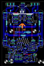
Im not sure my PCB layout is optimal, but I had to work hard to fit two channels into a 160x120mm board. Surface mount would help I guess, but my hands arent that steady I have put the PCB layout here.
I usually do use 22K feedback and input impedance. Why? Hm, well I started learning from Rod Elliot's stuff, and just stuck with it
I think it's a nice balance between not too noisy and not too low. It'll be driven by an opamp buffered volume control anyway.Im not sure my PCB layout is optimal, but I had to work hard to fit two channels into a 160x120mm board. Surface mount would help I guess, but my hands arent that steady
I have put the PCB layout here.Surface mount would help I guess, but my hands aren't that steady
Your hands don't need to be that steady. You hold the component in a pair of tweezers and rest your hand on the PCB, table etc to support it and to stop it shaking around.
With regards to your PCB, I guess you will be applying power to the boards at C113/C114?
I am also wondering why you chose to use an output triple if you're only using a single pair of output transistors. In your original schematic, I had assumed that you'd omitted the extra pairs for clarity
Of course if this is because you want to try a triple then there's nothing wrong with that either.Are you going to be adding a protection circuit on another board, or just not bother with one?
You might have to break R129 and use a separate return to the star point from J105 instead, but that shouldn't be too much of an issue. I can see that you've placed the ground trace and components with some care, it will be interesting to see if you get any trouble from the decoupling ground bleeding into the signal ground.
I have also edited the PCB in paint a little, well added a small change that might help. Basically at the midpoint between the RE resistors, move the trace where I've highlighted in orange and then create a T off of it and attach the down bit to the output inductor and then attach the feedback point to the small trace beneath the output inductor.
Everything else looks fine.
Attachments
Your hands don't need to be that steady. You hold the component in a pair of tweezers and rest your hand on the PCB, table etc to support it and to stop it shaking around.
With regards to your PCB, I guess you will be applying power to the boards at C113/C114?
At J101/102, but yes. Fuses will be on the board with the main supply capacitors, shown here
I am also wondering why you chose to use an output triple if you're only using a single pair of output transistors. In your original schematic, I had assumed that you'd omitted the extra pairs for clarity
Mainly because I wanted to try it. The particular configuration here I saw in Roender's take on the symasym, and thought it'd be interesting. Straightforward CFP has put me off in the past due to oscillation issues.
Are you going to be adding a protection circuit on another board, or just not bother with one?
Will have a separate DC protect board, but no VI limiting. It will be a personal amp used in my office at average volume so it won't be abused
You might have to break R129 and use a separate return to the star point from J105 instead, but that shouldn't be too much of an issue. I can see that you've placed the ground trace and components with some care, it will be interesting to see if you get any trouble from the decoupling ground bleeding into the signal ground.
Well the beauty of it is I can, if necessary, simply not fit R129 and take a separate wire back to star ground as you mention
I have also edited the PCB in paint a little, well added a small change that might help. Basically at the midpoint between the RE resistors, move the trace where I've highlighted in orange and then create a T off of it and attach the down bit to the output inductor and then attach the feedback point to the small trace beneath the output inductor.
Everything else looks fine.
Yes, that is a good idea. Good to know my PCB design doesnt totally suck
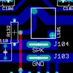
Not quite, move the inductor down so it also connects a little into the T. From what I understand there are currents that flow between the output devices that don't flow into the speakers, you obviously don't want the inductor to be in that path and you don't want any of these influencing the feedback path. These currents aren't present in a class A amplifier, as there is always a constant current flowing through the power devices.
Really though from a PCB design stand point it isn't hard to design one, especially for a lower powered design, you just have to know what to and not to do.
1) Have separate ground returns for the decoupling and signal grounds. You may connect the VAS transistor to the decoupling ground without performance degradation.
2) At the point where the traces coming from the RE resistors meet, take a T off and connect the output inductor to this and take the feedback point just after the inductor if possible.
3) Make sure that no high current traces run close to or parallel to any of the input stage circuitry. If you've got the power coming in via wires, this gives you flexibility with regards to reducing induction based distortion. If everything is combined on a PCB, you don't, this is where I feel having the power traces flanking the ground return trace is probably far more beneficial.
4) Have the power come in close to the power transistors. Have the power trace feed into the power transistors then, to power the rest of the amplifier take a trace after the transistors. What you don't want to do is feed power in at the input stage and then have those traces feeding the output transistors, this makes large currents flow through the traces around the input circuitry and won't be a good idea.
5) Keep the input stage circuitry as far away from the output stage as possible
That's essentially what I did when designing my PCBs, for both this amplifier and the low powered one linked to at the start of the thread. Where signal traces and power traces are close together, I tried to take them to different sides of the PCB if possible, obviously you can't do that with a single sided PCB.
When it comes to where do you feed the ground return for the current sources? I think that it's best to run these through the signal ground. They do not contain contaminants and are probably beneficial.
With class A biasing, decoupling currents and induction based distortion cannot harm the performance. This is because the current flowing in the power rails is constant. As a result, regardless of the signal being amplified the current drawn is always the same.
In class AB amplifiers, half sine wave pulses develop on the power rails because current demands are placed on the power rails that vary in proportion to the magnitude of the signal being amplified.
If there is a constant current flowing through the signal ground, it might be harder to pollute it? This might be total rubbish mind you, as you've still got half sine wave pulses on the supply rails.
I guess to test this I could feed a large current through the signal ground from my bench power supply and see if it affects the induction distortion.
Last edited:
I thought I'd just add in that a simple VI limiter isn't hard or really that complicated to add in. It costs just a few pence too. If you can find the board space just add one in, even if you choose not to use it. If you're using the typical fare of output transistor sc5200/sa1943 etc you can see values for one in my other blameless thread.
You might think that you will never do anything that blows the amp up, but you'd be surprised how often you can do stupid things And I know its only a case of replacing the output transistors and the fuses and, well you will need to unscrew the board from the heat sink, reset the bias, check for shorts between the trannies and the heat sink. I'd rather have the amplifier short circuit proof If you find space is really at a premium you could try using some surface mount parts. You should be able to fit the circuit either side of the output inductor, in the area you've got marked up for screw holes I think. In that area you've got easy access to the power rails and the output of the amplifier, the only other thing you need is the bases of the drivers, which shouldn't be too hard, even if it needs to be a wire link.
You might think that you will never do anything that blows the amp up, but you'd be surprised how often you can do stupid things
And I know its only a case of replacing the output transistors and the fuses and, well you will need to unscrew the board from the heat sink, reset the bias, check for shorts between the trannies and the heat sink. I'd rather have the amplifier short circuit proof If you find space is really at a premium you could try using some surface mount parts. You should be able to fit the circuit either side of the output inductor, in the area you've got marked up for screw holes I think. In that area you've got easy access to the power rails and the output of the amplifier, the only other thing you need is the bases of the drivers, which shouldn't be too hard, even if it needs to be a wire link.Another method:
Interpose a 1M resistor between inv and non-inv inputs. Call it Rt.
Input 1Vp into the circuit from the signal source.
Measure output, let us say it is 25Vp, and a current probe (LTSpice) across Rt indicates 25nAp is flowing. This means there is 1M x 25nA = 25mVp across the test resistor.
Open Loop gain is 20log(Vout/V(Rt)), in this case 20log(25/0.025), viz 60dB.
If Closed Loop Gain (Av) is 28dB, then Loop gain must be 32dB.
1M is generally high enough to ensure very little measurement error.
Hugh
Hey guys, you don't have to add dummy parts to plot a differential voltage in LTspice. Select one node, then right click the plot label; edit the formula like (V(n019)-V(n020))*100. And by multiplying small voltages or currents, you can see their relationship to larger ones on the same plot.
Cheers,
Steve
- Status
- This old topic is closed. If you want to reopen this topic, contact a moderator using the "Report Post" button.
- Home
- Amplifiers
- Solid State
- Beefing up the Blameless.