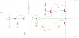
The basic topology looks OK. I would say that emitter resistors on the output devices are madatory for thermal stability. 0.22 or 0.33 ohm would be suitable. Also consider adding resistors across the base/emitter junction of each output device. Something in the region of 220 ohm. The feedback return resistor could do with being AC coupled too to improve DC stability and offset. A small cap (say 10uf) across Q3 would be beneficial too.
As with anything, you can tweak tweak tweak but the resistors mentioned are essential, the AC coupling of feedback desirable.
Also add a zobel network at the output consisting of a 0.1uf and 10 ohm in series to ground. You might well need a small (say 15pf) cap across R5.
Why not simulate it ?
As with anything, you can tweak tweak tweak but the resistors mentioned are essential, the AC coupling of feedback desirable.
Also add a zobel network at the output consisting of a 0.1uf and 10 ohm in series to ground. You might well need a small (say 15pf) cap across R5.
Why not simulate it ?
OK thanks mooly. The high power Dicker amp does not use emitter resistors on the outputs so not sure they are required?
The input is AC coupled to stop base currents going through the volume pot that will increase DC imbalance and cause a nasty crackle as the pot is turned. The tail current is very low @ 1/2 mA and the ground resistor small @ 10k - so there should be very little DC offset as long as the LTP transistors are well matched which I will do. that is why I think I can get away DC grounding the feedback node. I really am looking to save every part I can.
thanks
Also consider adding resistors across the base/emitter junction of each output device. Something in the region of 220 ohm.
That will definitely improve performance, but then the drivers will probably be running too hot.
The amp is indeed about as simple as possible. It will sound fair, much room for improvement.
That is what I'm counting on. I will mount the bias spreader to the backside of an output transistor and hope for the best. Remember the original Dicker design used just a simple diode string with no part of it in thermal contact! No emitter resistors on the high power version either!! 100's built here in Australia...
My thoughts exactly.Why not build a chip amp if simplicity is the main requirement.
As often as this DIGI 125 design comes up for scrutiny, it gets roundly criticised for being too simple, overtaxing the puny drivers, lousy bias setting etc. but it was used in quantity and for several power levels up to 200W over many years by the author, in a professional capacity.
I realize that the circuit's performance claims may seem far fetched as I thought too, but I built 4 of them back in the day (operating with the specified Motorola TO3s and Philips TO92s) and they all behaved themselves and made quite good 50W powered speakers for PA use. Even with simple diode biasing, they could take quite a hammering without instability or undue failures if you were careful with input level and used plenty of heatsinking.
It actually sounded good for a cheap design. In fact, so good that the AKSA 55 was inspired and largely based on it. I would not try to soup up the basic design simply by fitting high Ft transistors like 2SC5200/A1943 though. For only 25W, TIP3055/2955 will be fine and tough enough there, if they are genuine ON-Semi or ST Micro parts. Otherwise, it may need a careful analysis and probably the additional complexity of more components to ensure it remains stable - much as already suggested, I would think.
chip amp projects don't interest me at all. You simply copy the datasheet design and job done.
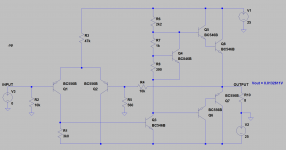
mooly - thanks for running this up in a sim. Maybe I should have done that myself but I think I have found the cause of massive DC imbalance. Please tell me if I am on the right track here...
If Q1 and Q2 are well matched then equal base currents will flow through R1 (10k ohm) and R4 (560 ohm). The problem is that different voltages will be developed across these different resistances throwing the diff amp out of balance. the solution is to increase R4 to 10k ohm to match R1 and to increase the feedback resistor to 180k ohm to maintain the original closed loop gain i.e. full power output at approx. 1Vrms input.
Ian - you make a very good point about the output devices I think. The high speed 30 MHz ft parts are going to be much more susceptible to stray inductance and parasitics than the 2 MHz ft parts Grahame used in his design. Probably one of the reasons why it gets away without the usual base stoppers, output zobel, etc. I will go find some TIP trannies on RS electronics.
I neglected to mention the work that member Greg Erskine put into a similar project called the "Baby AKSA" or "B-AKSA" amplifier. This shows pretty well how to upgrade the basic Digi design, incorporating the improvements discussed and more. Others may find some interesting comments and findings, if you've already seen his web pages and thread here:
http://www.diyaudio.com/forums/solid-state/168554-based-hugh-deans-aksa-55-a.html
Greg's Web Site
http://www.diyaudio.com/forums/solid-state/168554-based-hugh-deans-aksa-55-a.html
Greg's Web Site
mooly - thanks for running this up in a sim. Maybe I should have done that myself but I think I have found the cause of massive DC imbalance. Please tell me if I am on the right track here...
If Q1 and Q2 are well matched then equal base currents will flow through R1 (10k ohm) and R4 (560 ohm). The problem is that different voltages will be developed across these different resistances throwing the diff amp out of balance. the solution is to increase R4 to 10k ohm to match R1 and to increase the feedback resistor to 180k ohm to maintain the original closed loop gain i.e. full power output at approx. 1Vrms input.
Looking at just the input stage, with 10k and 560 ohms (R1 and R4) the currents are still not exactly equal... close but still unequal. Perhaps 15 to 20% difference and that is with absolutely matched devices, which in simulation they are. Edit... that is looking at the input stage in isolation i.e. not connected to the rest of the amp.
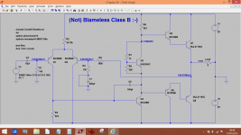
By making R2 variable you can trim the offset to zero but its all a poor way of doing things. The amp is just to simplistic to endorse. Having no zobel network means oscillation and instability is more likely than not as soon as a real load is connected. That even shows in simulation as you can see.
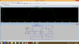
Squarewave response at 25kHz is not good for several reason.
(hope Doug doesn't see what his blameless amp has turned into
")
Attachments
I neglected to mention the work that member Greg Erskine put into a similar project called the "Baby AKSA" or "B-AKSA" amplifier. This shows pretty well how to upgrade the basic Digi design, incorporating the improvements discussed and more. Others may find some interesting comments and findings, if you've already seen his web pages and thread here:
http://www.diyaudio.com/forums/solid-state/168554-based-hugh-deans-aksa-55-a.html
Greg's Web Site
http://anistardi.wordpress.com/2014/04/19/aksa-55-dalam-simulasi/
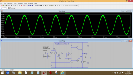
I mucked around in ltSpice for a while to test my theory about increasing the feedback resistor and it actually made things worse. After playing with some different values the best DC offset was when the feedback resistor is equal to the input ground shunt or thereabouts.
With a little fine tuning of the LTP collector I get 15mV offset which is pretty darn good all things considered. Obviously real world won't be as good but as long as it sits +/- 150mV it will suit my purposes.
I know people are going to poo poo this design... but i'm not looking for anything hi-fi just something that plays music in my bedroom though a pair of cheap speakers through 20cm of figure 8 wire. If Graham was able to sell this in the 100's why wouldn't it work??
Attachments
I can't comment on the original design that yours is based on without seeing a full diagram.
Your sim... the offset simulates as quite low, its actually nearer 85mv than 13mv (there's a simple error in your sim)
What you must remember is that the sim uses 100% matched devices. Throw in something else for just one of the input devices and the offset is closer to 1 volt.
We all learn through building and experimenting so I would say go ahead, keep the bias low and see how you get on.
Your sim... the offset simulates as quite low, its actually nearer 85mv than 13mv (there's a simple error in your sim
)What you must remember is that the sim uses 100% matched devices. Throw in something else for just one of the input devices and the offset is closer to 1 volt.
We all learn through building and experimenting so I would say go ahead, keep the bias low and see how you get on.
- Status
- This old topic is closed. If you want to reopen this topic, contact a moderator using the "Report Post" button.
- Home
- Amplifiers
- Solid State
- based on Graham Dicker DIGI amp