Yes mooly removing the feedback ground shunt cap (DC coupled) means that the offset moves around as the signal amplitude changes i.e. hot and cold.
Its not jumping around as might be expected if the amp is oscillating. All transistors (except VA) are cool to touch at idle.
Removing that cap may well cause instability at really high frequency, you would need to put a scope on it and confirm (or otherwise) that there is a problem.
Ok thanks mooly I will have another look at the scope trace tomorrow (it is late here now).
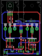
I want to etch some proper boards because what I have at the moment isn't ideal - flyleads between the PCB and outputs mounted on heatsink. I think I will put some base resistors on the outputs until I get make a proper PCB.
I want to etch some proper boards because what I have at the moment isn't ideal - flyleads between the PCB and outputs mounted on heatsink. I think I will put some base resistors on the outputs until I get make a proper PCB.
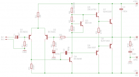
The downside to compactness is inductive and capacitive coupling between the input stage and the output. That couples power supply ripple into the signal and results in distortion - not the sweet, mellow H2 type either. In my limited PCB experience with making distortion comparisons, a bit more space between these nodes is a good idea for power amplifiers..... Any comments?....layout is 2x2" so nice and compact to keep parasitics to a min.
If you aren't too fussed with refinements, just build as you have drawn and consider improving it as you progress from mk1-mk2-mk99 etc.

re: suck-out (or speed-up) caps. This definitely refers to the output transistors. They cannot lose stored base charge fast enough for the signal's rate of change around the crossover point. The cap provides a faster discharge path in EF designs but tough luck for CFP (complementary feedback pair) designs - they remain problematic.
You'll find this better explained with graphs and figures in section 5.3 referred to earlier.
thanks guys for taking the time to cast your eye over the board.... Ian you make a good point about coupling of the half wave high currents coupling with the sensitive small signal traces. I definitely want to refine and obsessively perfect the layout because I think this is going to be far more important to getting a good result than coming up with some fantastically complex schemat that in theory (ltSpice) is 0.00000001 % thd but in practice is a dud because of bad layout. I'm going to add an extra inch or so to the PCB and revise the layout tonight.
I am really nervous about the idea of a cap to suck out base charge. I see the benefit it brings to the table BUT.... that stored charge has to go somewhere, sometime, and to my thinking it has the potential to seriously upset the bias when it does. I will think on it some more.....
I am really nervous about the idea of a cap to suck out base charge. I see the benefit it brings to the table BUT.... that stored charge has to go somewhere, sometime, and to my thinking it has the potential to seriously upset the bias when it does. I will think on it some more.....
Last edited:
Perhaps just unfamiliar with the feature. It has been an integral part of many BJT switch designs for decades but for emitter follower output stages, a cap. is not strictly necessary if you are using more robust drivers with higher driver bias currents or simply not chasing the shortest switch-off delay...I am really nervous about the idea of a cap to suck out base charge. I see the benefit it brings to the table BUT.... that stored charge has to go somewhere, sometime, and to my thinking it has the potential to seriously upset the bias when it does. I will think on it some more.....
Clean switching performance is required for good class AB so if you want to use high Ft parts, their higher switching speed demands addressing this limitation - otherwise they're wasted, only contributing to instability. For more on how the cap helps, Google brings up a number of references including some helpful posts here. Try "Transistor base suck-out capacitor" and follow the trail.
As said by others, there are worse problems here. The need to fix them depends on whether you are committed to the raw, elemental OP design or you want to continue modifying it as you see the technical benefits emerge in discussion.
You will likely wind up with yet another generic design by continuing to improve the Digi but I would still read all of Self's distortion paper or book and study the features of the blameless design first, followed by more complex and higher power designs with the format of the Leach amplifier, favoured by US DIYs and authors such as Bob Cordell. There are older ideas for simple, good sounding amplifiers too...

You are quite right I am unfamiliar with this feature and unfamiliar with power stages in general....
But the more I think about this the less and less I like the idea of this suck out cap. in order for it to do a good job of quickly pulling out the base charge it is going to have to be a fairly large part (examples I'm seeing are between 470n and 1u). The time constant of the cap is going to be working against the emittter res so and in theory it could hold a stored charge some time well after that event.
So better solutions:
1. brute force solution involving large TO220 Power trannies capable of heavy Class A operating range via a very low value emitter res that will very effectively reverse bias the output bases.
2. the more elegant solution perhaps (but high parts count) would be to drive the outputs from current sources and control the turn off (rather than turn on) with folded drivers. I saw this technique used on a Power MOSFET design, presumably to overcome the substantial gate charge and maximise the speed of these devices.
I guess my main concerns are:
a) if I not worry about the speed up cap am I simply accepting higher HF distortion or;
b) the more ominous conclusion in this article is that it also reduces conduction at HF which could make it difficult to push up the ULGF to take advantage of the 30 mhz parts.
any experts around have any experiences to add?
It doesn't seem appropriate to focus on this one possible design refinement when the fundamentals are still in dire need of improvement, as Mooly has pointed out. After all, it's a cheaper than cheapo utility amplifier, not a hi-fi design to begin with. I don't see any problem with a 1uF 63V MKT cap. but if you intend to use SMT, suitable parts for many typical amplifier designs may prove difficult to source.
Build as originally designed again, with room for your modifications. Then alter it according to your plan and test, listen, verify results. I still suggest you don't use high Ft parts until stability proves very good, which means not with the Digi design as it is. In any case, an analog oscilloscope will be essential for checking this out and for properly investigating almost any audio design.
Build as originally designed again, with room for your modifications. Then alter it according to your plan and test, listen, verify results. I still suggest you don't use high Ft parts until stability proves very good, which means not with the Digi design as it is. In any case, an analog oscilloscope will be essential for checking this out and for properly investigating almost any audio design.
I've been hunting around the datasheets looking for suitable TO126 or TO220 packaged driver transistors available through the local RS distribute. Getting a good mix of package Pd and Ic, along with respectable ft and hfe is no easy feat and most of the good ones seem to be discontinued or not available here in Australia.
The MJE15032/33 look pretty reasonable. Speed and gain are lower than I would like in this application but at least I'll never have to worry about beta droop!
So I'll sub the drivers with these parts and bias em HOT HOT HOT at about 100mA (27 ohm emitter res). No cap..... but if charge suck out is a prob I will eat my hat...
thanks Ian
BD139/40 are fine for even 50W with Vceo 80V, Icmax 1.5A. You don't need 8A capability from drivers until working with 150-400W amplifiers and considering your present ones are only naked TO92s, it will take a lot of excess bias current to approach even the BDxxx pair's peak current rating. In class A mode with virtually constant dissipation, driver beta droop is unlikely to be a concern as it is with class AB output devices. Fit heatsinks suited to 3W dissipation and let's learn to walk before running wild with ideas.
Not sure what circuit you refer to now but consider that reducing Re to increase bias, also increases AC drive loss to the output transistors. Start around 47Ω and verify you have full output voltage up to full power into a resistive load. Simulate and/or test properly up to full power when making radical changes like this without precedent.
BTW, Hats are an acquired taste but you get used to eating them around here. The humble pie for seconds isn't so bad though.
BTW, Hats are an acquired taste but you get used to eating them around here. The humble pie for seconds isn't so bad though.
Lol
 very true. I've just had to do that in another thread
 BD139/40 are fine for even 50W with Vceo 80V, Icmax 1.5A. You don't need 8A capability from drivers until working with 150-400W amplifiers and considering your present ones are only naked TO92s, it will take a lot of excess bias current to approach even the BDxxx pair's peak current rating. In class A mode with virtually constant dissipation, driver beta droop is unlikely to be a concern as it is with class AB output devices. Fit heatsinks suited to 3W dissipation and let's learn to walk before running wild with ideas.
Not sure what circuit you refer to now but consider that reducing Re to increase bias, also increases AC drive loss to the output transistors. Start around 47Ω and verify you have full output voltage up to full power into a resistive load. Simulate and/or test properly up to full power when making radical changes like this without precedent.
BTW, Hats are an acquired taste but you get used to eating them around here. The humble pie for seconds isn't so bad though.
Crikey Ian!! first the drivers were too small now they're too big... I can't win
Well I'll give the 2sa1837/2sc4793 a go instead. Not as beefy as the MJE's (20w vs 50W) but much nicer specs otherwise.I was poking around with the DIGI prototype and ended up killing a TIP tranny accidently shorting the output while load testing.... thinking about adding short circuit protection to the board too since mistakes happen when hooking up speakers
edit; scratch that just came across KSA1220/ksc2690 they look like just what i need
Attachments
Last edited:
I didn't realise you were lurking here Ranchu - good to see you. Bobma shops at RS, IIRC, and like other local sellers, their stock range of audio parts is woeful - as you might expect when most are now obsoleteCrikey Ian!! first the drivers were too small now they're too big... I can't win
The direction of the thread has changed a bit since we began. Presently, it's at "hot hot hot" driver bias in lieu of suck-out caps. We started with teensy BC546/56, but there is little choice going up from there when we are using local suppliers.
However, for driver experiments, I don't see any need yet for exotics nor waiting weeks for deliveries. I don't even think there is going to be a need for such techniques at this low power level but the BDs (Fairchild or ST Micro are reasonable ) will do fine to demonstrate any advantage in high bias whilst ever there is real risk of smoking parts in the wobbly circuit. Simulation would prove this much quicker of course, but sometimes we may need to see the physical assembly and hear it working in some fashion too.
I didn't realise you were lurking here Ranchu
 He was posting here as bobma. Forum rules prohibit multiple registrations, so he can keep things simple by not pretending to be two different people.
- Status
- This old topic is closed. If you want to reopen this topic, contact a moderator using the "Report Post" button.
- Home
- Amplifiers
- Solid State
- based on Graham Dicker DIGI amp