mooly you are right about the DC offset. Even when the ground resistances are near identical at the non-inverting and inverting inputs - R1 = (R4 || R5) and the LTP collector resistor is properly defined the DC offset will change considerably once sim "real world" mismatch between Q1 and Q2, thermal drift , etc.
I'm not going to abandon this completely yet. I think with some careful matching of Q1 and Q2 and good thermal coupling (zip tied back to back) the problem is managable.
Why is so much fuss made about offset anyway? I mean even 250mV is only 8mW through an 8 ohm speaker - hardly any power and certainly not enough to cause damage.
It would be better to breadboard the Digi amplifier and get a grip on reality before you find yourself on a Spice driven path to a generic Lin-Thompson amplifier anyway. Spice is certainly fast and good for specs - but do you always need them? Why not listen, measure and find out?.....Why is so much fuss made about offset anyway?.....
Low DC offset has certainly become more fashionable whereas is years gone by offsets of 100mv were considered acceptable.
The big worries with your design are stability due to it having no zobel network and output inductor, and a tendency to thermal runaway at anything other than well below optimum bias levels.
The big worries with your design are stability due to it having no zobel network and output inductor, and a tendency to thermal runaway at anything other than well below optimum bias levels.
I built a couple of these amp modules using PCBs supplied by the author in my late teens when it was first published in ETI. The SQ was extremely disappointing. They went in the bin not long afterwards. Now I understand more about amp design I realise why. Quite frankly I find it hard to believe most of what the author wrote about it in that article. The only thing it had going for it was a small board and few components. Small board is nice, but these days SMD components are the way to achieve this, and using fewer components really is an insignificant cost saving when they are Rs and small BJTs, especially for hobbyists.
If you want to build a Lin topology amp, go for one that's been designed properly such as Self's Blameless or Silicon Chip's version of it, the ULDmkIII (now mkIV coming) or Rod Elliot's P3A, and do it properly. There are good boards available for all these - the board is half the design after all. Even if your application is uncritical, why waste time on a design that's fundamentally flawed? If you go with any of the above, at least you're starting with something that works properly as is and can then be tweaked if you think the SQ is lacking. Or better still try some other topologies... Silicon Chip's SC480 and Studio 350 sound better to me. Interestingly they are based on the original Hitachi MOSFET application note circuit with differential VAS, a configuration that is dismissed by Self and others, but they sound better to me.
Even if its simplicity appeals to your "inner Zen" or whatever, I think this design is simpler than it needs to be.
I built a couple of these amp modules using PCBs supplied by the author in my late teens when it was first published in ETI. The SQ was extremely disappointing. They went in the bin not long afterwards. Now I understand more about amp design I realise why. Quite frankly I find it hard to believe most of what the author wrote about it in that article. The only thing it had going for it was a small board and few components. Small board is nice, but these days SMD components are the way to achieve this, and using fewer components really is an insignificant cost saving when they are Rs and small BJTs, especially for hobbyists.
If you want to build a Lin topology amp, go for one that's been designed properly such as Self's Blameless or Silicon Chip's version of it, the ULDmkIII (now mkIV coming) or Rod Elliot's P3A, and do it properly. There are good boards available for all these - the board is half the design after all. Even if your application is uncritical, why waste time on a design that's fundamentally flawed? If you go with any of the above, at least you're starting with something that works properly as is and can then be tweaked if you think the SQ is lacking. Or better still try some other topologies... Silicon Chip's SC480 and Studio 350 sound better to me. Interestingly they are based on the original Hitachi MOSFET application note circuit with differential VAS, a configuration that is dismissed by Self and others, but they sound better to me.
Even if its simplicity appeals to your "inner Zen" or whatever, I think this design is simpler than it needs to be.
This amplifier is simple but performance is enough
")
Yes , convince him to go the stable EF2 route - no darlington.
OS
OS, this is simple amplifier. Of cource EF3 will be better
OS, this is simple amplifier. Of cource EF3 will be better
I did not say to go EF3 ? Keep it simple , even an EF2 with 2 diodes and
a trimmer is better than darlingtons.
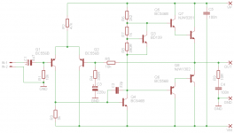
Zener-resistor current source , LTP , VAS/bootstrap , EF2 (4 devices).
A 7 transistor "good little amp" .. that's all. Add a real bias spreader -8 ,
red led current source -9 .
OS
It would be better to breadboard the Digi amplifier and get a grip on reality before you find yourself on a Spice driven path to a generic Lin-Thompson amplifier anyway. Spice is certainly fast and good for specs - but do you always need them? Why not listen, measure and find out?
Once TIP transistors arrive from RS i will do just that. I want to make a couple of tweaks to make it my own.
Low DC offset has certainly become more fashionable whereas is years gone by offsets of 100mv were considered acceptable.
The big worries with your design are stability due to it having no zobel network and output inductor, and a tendency to thermal runaway at anything other than well below optimum bias levels.
Built a few amps most without output inductor and they were fine. you have me worried about the Zobel but the original DIGI had none with the slow old TIP transistors so maybe ok??
I built a couple of these amp modules using PCBs supplied by the author in my late teens when it was first published in ETI. The SQ was extremely disappointing. They went in the bin not long afterwards. Now I understand more about amp design I realise why. Quite frankly I find it hard to believe most of what the author wrote about it in that article. The only thing it had going for it was a small board and few components. Small board is nice, but these days SMD components are the way to achieve this, and using fewer components really is an insignificant cost saving when they are Rs and small BJTs, especially for hobbyists.
If you want to build a Lin topology amp, go for one that's been designed properly such as Self's Blameless or Silicon Chip's version of it, the ULDmkIII (now mkIV coming) or Rod Elliot's P3A, and do it properly. There are good boards available for all these - the board is half the design after all. Even if your application is uncritical, why waste time on a design that's fundamentally flawed? If you go with any of the above, at least you're starting with something that works properly as is and can then be tweaked if you think the SQ is lacking. Or better still try some other topologies... Silicon Chip's SC480 and Studio 350 sound better to me. Interestingly they are based on the original Hitachi MOSFET application note circuit with differential VAS, a configuration that is dismissed by Self and others, but they sound better to me.
Even if its simplicity appeals to your "inner Zen" or whatever, I think this design is simpler than it needs to be.
All good comments and I have built Rod's amp and the blameless. My recollection of the DIGI 125 is not as bad as you say but that was about 20 years ago so hard to remember.
First one I built 7 years ago. So happy it worked back then.
.asc and the LT models are below , too.
OS
ostripper what is an "EF2" and "EF3". Are you referring to the emitter follower output stage in your schematc? there are a lot of parts here relative to the performance I think..... Do you really need all those base stoppers to make this stable? Maybe the board layout is no good... Also you are using TO220 Power transistors as drivers. Great.... no beta droop at high power but with the low beta at all levels it is really going to load up the VA stage which..... does not have much standing current.
Don't be concerned about the gain linearity of those MJE150XX drivers. They're a few notches above a TIP41/42 or similar pairs and you may note they are used in SC's ULD amplifiers too. Toshiba's best drivers are also TO220, FWIW. They may be overkill for a low power amplifier but the limited number of decent TO126 drivers now, is a bigger problem..... Also you are using TO220 Power transistors as drivers. Great.... no beta droop at high power but with the low beta at all levels it is really going to load up the VA stage which..... does not have much standing current.
The EF2 and EF3 terms used here, are shorthand for a single cascaded Emitter follower and double cascaded emitter follower output stages respectively. Simply put, there are 2 complementary stages in EF2 and 3 in EF3.
Douglas Self designates EF2 as simply EF and uses EFII to mean an improved form, incorporating a base charge "suck-out" cap. If you don't have one of his "Audio Power Amplifier Design Handbook" editions, see section 5.3 fig 13 here for illustrations using his terminology: Distortion In Power Amplifiers
I'm back!!!!
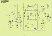
So the TIP trannies arrived and I finished putting it all together. To start with close to the original DIGI schem.... with most of the parts on protoboard and the output trannies bolted to a heatsink and the bias spreader bd139 on the back of the NPN one. the only differeces..... 25V rails, input cap in circuit, no emitter resistors , and my bias spreader from post 1 in place of the diode string.
After fixing up some wiring probs it passes a pretty clean sine wave into a resistor load. DC offset is about 100mV even with the input and feedback caps in place..... No idea why Graham chose the values he did... replaced the input ground and feedback resistors with 10k and -IN ground res 470r, LTP collector res to 3.3k and offset is down to 10mV. not too shabby with unmatched transistors.
Tried pulling out the feedback cap.... well it works but the offset jumps around depending on temp and at one point was over 150mV. That much doesnt worry me but what does is how much it jumps around. Maybe it hits 500mV under some conditions and that would be a prob for sure. So Mooly you were right - i don't think it is worth the drama just for the sake of one small cap.
I think the sound is good with small cheap speakers I'm using. And I'm sure it could be improved with better more modern parts.
Going to etch some PCBs and experiment with the faster 30mhz onsemi trannies and maybe one or two other tweaks.
Attachments
Don't be concerned about the gain linearity of those MJE150XX drivers. They're a few notches above a TIP41/42 or similar pairs and you may note they are used in SC's ULD amplifiers too. Toshiba's best drivers are also TO220, FWIW. They may be overkill for a low power amplifier but the limited number of decent TO126 drivers now, is a bigger problem.
The EF2 and EF3 terms used here, are shorthand for a single cascaded Emitter follower and double cascaded emitter follower output stages respectively. Simply put, there are 2 complementary stages in EF2 and 3 in EF3.
Douglas Self designates EF2 as simply EF and uses EFII to mean an improved form, incorporating a base charge "suck-out" cap. If you don't have one of his "Audio Power Amplifier Design Handbook" editions, see section 5.3 fig 13 here for illustrations using his terminology: Distortion In Power Amplifiers
thanks Ian for this info and for your encouragement. I don't understand this "speed up cap" talked about in the article. Surely the optimal value is going to depend on the rate of change and magnitude of the driver current i.e. both frequency AND amplitude dependent with are highly variable parameters! That stored charge has to go somewhere and is most likely going upset the bias conditions when it is the 'wrong' value (which it almost always will be). If we are using huge TO220 drivers then just heatsink and bias 'em hot.
Are you sure we are not confusing the bias spreader bypass cap that is very useful to make sure the amplified diode only sees DC?
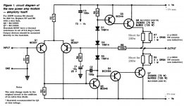
Ok now that the basic circuit is working I've made a couple of tweaks that I'd like to try out...
first of all we have the lovely ONsemi sustained beta Power transistors that will put a lighter load on the teeny drivers and and better VA stage Zin. These parts have a 30mhz BW product vs. the rather shabby 2mhz for the TIP parts in DIGI 125. So.... we should be able to push up the ULGF and I'm shooting for 1.25 mhz with a good layout. I think the Graham design is only about 350 khz from memory so THD won't be great.
The only other changes.... I've now set the Pmax for 600mV input to better suit the MP3 player's max Vout.
Zobel network provided for..... I'm nervous the fast ONsemi parts will be more difficult to tame.
Attachments
It sounds like it could be unstable at HF/RF if removing the feedback cap causes the bias to jump around. Do you mean the feedback return electrolytic, C1 in your latest diagram ?
Removing that cap (running it at unity gain) would see instability.
Yes mooly removing the feedback ground shunt cap (DC coupled) means that the offset moves around as the signal amplitude changes i.e. hot and cold.
Its not jumping around as might be expected if the amp is oscillating. All transistors (except VA) are cool to touch at idle.
- Status
- This old topic is closed. If you want to reopen this topic, contact a moderator using the "Report Post" button.
- Home
- Amplifiers
- Solid State
- based on Graham Dicker DIGI amp