Hi HarryDymond !
You try to disconnect your pre-amp and test your power amp . You try to connect zobel circuit to right of choke .
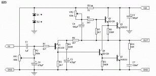
You try to increase C6 and C7
I have no problem with normal darlington . With triple darlington , my amp is also unstable . I also use stopper resistor for output tst . It is helpful for stable but it increase distortion .I only use 1 ohm stopper resistor .
I dont use R15 , only use C3 .
a big C3 can decrease ocsilation but increase TIM with complex load
You try to disconnect your pre-amp and test your power amp . You try to connect zobel circuit to right of choke .
You try to increase C6 and C7
I have no problem with normal darlington . With triple darlington , my amp is also unstable . I also use stopper resistor for output tst . It is helpful for stable but it increase distortion .I only use 1 ohm stopper resistor .
I dont use R15 , only use C3 .
a big C3 can decrease ocsilation but increase TIM with complex load
Eva wrote:

Again, have a look to Solomon: The worst effect occurs, when the amplifier operated with capacitive load ... Load capacitance for the output follower cause it to have negative input conductance, while the driver follower can have inductive output impedance. These components combine with the capacitance of interstage to generate the equivalent of a one-port oscillator.
Fig.25
The base stopper purpose is to prevent the previous stage from being loaded with a _negative_ impedance from the output follower.
Concerning base stopper resistors, my point of view is that their purpose is to prevent the previous stage from being loaded with a too capacitive impedance from the next stage, that otherwise could cause instability. For example, a VAS with some miller capacitance may be made instable by loading it directly with some capacitor value.
Again, have a look to Solomon: The worst effect occurs, when the amplifier operated with capacitive load ... Load capacitance for the output follower cause it to have negative input conductance, while the driver follower can have inductive output impedance. These components combine with the capacitance of interstage to generate the equivalent of a one-port oscillator.
Fig.25
The base stopper purpose is to prevent the previous stage from being loaded with a _negative_ impedance from the output follower.
Hi, Dimitri,
Thanks for the advice. It is really a very good paper, not to difficult to read, with many knowledge inside. For example I got a clue about chip manufacturers, why they make chips like LM3886 or LM3875 a quasi-complementary output stage.
The pole splitting in this paper seems to concentrate with topology with current mirror in the differential, and CCS loaded VAS, where R1 about 1.7Mohm, R2 about 100Kohm.
Is this paper still holds for topologies like Citation12? Where the differential is R loaded (390ohm, not current mirror), VAS is bootstrapped (3k9+5k6+50uF), not CCS loaded.
http://web.mit.edu/klund/www/papers/ACC04_opcomp.pdf
is still very technical but gives a slightly different explaination of miller compensation "pole splitting"
vas output z from the simple circuit model won't show the utility of base stoppers, they control/damp oscillations from the emitter follower's internal local feedback transfroming the output C load at the emitter output terminal to negative input R at the emitter follower's base at frequencies where hfe is rolling off, the Intusoft newsletter I pointed to earlier tries to explain this
Hi, JCX,
Thanks for the link. I will study it, it seems too heavy for me, though .
.
Knowing that so many clever papers is made about 1 miller compensation, it shows that this problem is well known, and the cure is already known for a long time.
I would like to think inside the "Black Box" (Janneman, don't be angry with me)
It is known that the cause of instability is 2nd order slope when approaching the unity gain, when it reaches 180deg or more within the unity gain, the whole system will be unstable because of positive feedback.
Why not trying to overcome one pole before unity gain (JCX's pointed paper seems to mentioned a zero within the loop, to make only 1 pole for the whole system), instead of introducing a dominant pole with miller cap, that forces only 1 pole at unity gain, pushing the 2nd pole outside the unity gain, but making the flat OL bandwith more narrow.
My bla..bla...bla...(don't be angry with me, I'm not EE) is like this.
The first point is : what is that a base stopper do? John Curl (and Dimitri above) said that it is to overcome a "negative base impedance" at certain frequency.
I imagine (my bla..bla..bla..) that "negative base impedance" is a situation where the base is not normal, reversed. For example, in NPN bipolar, normally, the base should be sucking current. In "negative base impedance" condition, I assume that this NPN base is "giving" current, instead of sucking current.
The next bla..bla..bla...
Why this NPN base is giving current? EVA's explenation is good. Transistor is only 3 legged device. It don't know what is happening to itself. It's base should be given a "discharging" mechanism, not only thinking about the appropriate "charging" mechanism, like calculating bias current.
(Like a good car manufacturer, should not only thinking about how to make a car can run so fast, without thinking about making a suitable braking system)
This "discharging" mechanism could be as simple as a suitable valued R between B-E, or as sophisticated as EVA's bipolar drive mechanism. The important thing is that the base should be given a proportional charge-discharge system.
Another bla..bla..bla..
Look at DartZeel schematic next door. It sounds good (I haven't heard at it, though). Why?
This DartZeel amp has a nearly complete charging-discharging mechanism. I think that is why it can reach 1Mhz bandwith, with so simple cct, yet it is a power amp (ie: capable of delivering quite big current in big voltage swing).
Having this big bandwith will be good for phase all over the first 20khz.
From the input stage. Signal is injected between base of Q1 and Q2. Q1 is PNP, Q2 is NPN, that will pretty much a "charging-discharging" mechanism, one base is giving current, the other base is sucking current. Balanced. This input should be fast without stability problem.
The next transistor. Q1+Q3 (also Q2+Q4) is making a diamond buffer. Diamond buffer is fast, because in the base of the right transistor (for example NPN here) lies another transistor's emitor with opposite polarity (example PNP here). The NPN base is sucking current, and the emitor of PNP also suck current. The emitor of PNP should be a "discharging" device for the base of NPN.
Moving to the next transistor. Q7 (VAS transistor). The question is, why Q7 is not driven directly from the collector of Q3, yet HD put an emitor follower buffer Q5? And why Q5 is NPN, not the same type as Q7 (like VAS input buffer in Doug Self book)?
I think HD is very smart here. Emitor of Q5 (NPN) is giving current. Base of Q7 (PNP) is also giving current. Emitor of Q5 becomes a "discharging" mechanism for Q7's base.
Plus a bonus, Q5 acts as a buffer for Q7.
Then jumps to the final stage. It is another diamond buffer. Like above explenation, a diamond buffer is a perfect "charging-discharging" couple. It should be fast, without many phase problem.
The interesting thing is D3 infront of Q11. It seems that this D3 works as a "charging" maintain-er, to give "turbo" classA for Q11-Q12. Discharging story is failed here.
The missing link in this DartZeel is R21-R22. They are base stoppers. Because Q9 and Q10 doesn't have a discharging mechanism, it seems base stoppers there is mandatory.
If my bla..bla..bla.. is working, then base stoppers R21-R22 should be able to be replaced by a B-E resistor at Q9-Q10, to give discharging mechanism. Maybe 470ohm there is enough.
I will try this. Whether a base stopper can be replaced by discharging mechanism.
(I've experiment this within a SMPS using IRFZ44, it needs about 100ohm resistor from G to S, to provice discharging path. 150R or 220R is not enough for IRFZ44. And it works. It shows that B-E discharging resistor needs to be value adjusted, according to the charge inside the base/gate ie: the transistor size).
Another bla..bla..bla..
DOGC (Widowmaker) seems to sound good too, becaue the final transistors are in full charge-discharge system (the polarity at 47ohm is continiously +/- --> -/+ all the time, making a complete discharge for each output transistor side)
Thanks for the link. I will study it, it seems too heavy for me, though
.Knowing that so many clever papers is made about 1 miller compensation, it shows that this problem is well known, and the cure is already known for a long time.
I would like to think inside the "Black Box" (Janneman, don't be angry with me
)It is known that the cause of instability is 2nd order slope when approaching the unity gain, when it reaches 180deg or more within the unity gain, the whole system will be unstable because of positive feedback.
Why not trying to overcome one pole before unity gain (JCX's pointed paper seems to mentioned a zero within the loop, to make only 1 pole for the whole system), instead of introducing a dominant pole with miller cap, that forces only 1 pole at unity gain, pushing the 2nd pole outside the unity gain, but making the flat OL bandwith more narrow.
My bla..bla...bla...(don't be angry with me, I'm not EE
) is like this. The first point is : what is that a base stopper do? John Curl (and Dimitri above) said that it is to overcome a "negative base impedance" at certain frequency.
I imagine (my bla..bla..bla..) that "negative base impedance" is a situation where the base is not normal, reversed. For example, in NPN bipolar, normally, the base should be sucking current. In "negative base impedance" condition, I assume that this NPN base is "giving" current, instead of sucking current.
The next bla..bla..bla...
Why this NPN base is giving current? EVA's explenation is good. Transistor is only 3 legged device. It don't know what is happening to itself. It's base should be given a "discharging" mechanism, not only thinking about the appropriate "charging" mechanism, like calculating bias current.
(Like a good car manufacturer, should not only thinking about how to make a car can run so fast, without thinking about making a suitable braking system)
This "discharging" mechanism could be as simple as a suitable valued R between B-E, or as sophisticated as EVA's bipolar drive mechanism. The important thing is that the base should be given a proportional charge-discharge system.
Another bla..bla..bla..
Look at DartZeel schematic next door. It sounds good (I haven't heard at it, though
). Why?This DartZeel amp has a nearly complete charging-discharging mechanism. I think that is why it can reach 1Mhz bandwith, with so simple cct, yet it is a power amp (ie: capable of delivering quite big current in big voltage swing).
Having this big bandwith will be good for phase all over the first 20khz.
From the input stage. Signal is injected between base of Q1 and Q2. Q1 is PNP, Q2 is NPN, that will pretty much a "charging-discharging" mechanism, one base is giving current, the other base is sucking current. Balanced. This input should be fast without stability problem.
The next transistor. Q1+Q3 (also Q2+Q4) is making a diamond buffer. Diamond buffer is fast, because in the base of the right transistor (for example NPN here) lies another transistor's emitor with opposite polarity (example PNP here). The NPN base is sucking current, and the emitor of PNP also suck current. The emitor of PNP should be a "discharging" device for the base of NPN.
Moving to the next transistor. Q7 (VAS transistor). The question is, why Q7 is not driven directly from the collector of Q3, yet HD put an emitor follower buffer Q5? And why Q5 is NPN, not the same type as Q7 (like VAS input buffer in Doug Self book)?
I think HD is very smart here. Emitor of Q5 (NPN) is giving current. Base of Q7 (PNP) is also giving current. Emitor of Q5 becomes a "discharging" mechanism for Q7's base.
Plus a bonus, Q5 acts as a buffer for Q7.
Then jumps to the final stage. It is another diamond buffer. Like above explenation, a diamond buffer is a perfect "charging-discharging" couple. It should be fast, without many phase problem.
The interesting thing is D3 infront of Q11. It seems that this D3 works as a "charging" maintain-er, to give "turbo" classA for Q11-Q12. Discharging story is failed here.
The missing link in this DartZeel is R21-R22. They are base stoppers. Because Q9 and Q10 doesn't have a discharging mechanism, it seems base stoppers there is mandatory.
If my bla..bla..bla.. is working, then base stoppers R21-R22 should be able to be replaced by a B-E resistor at Q9-Q10, to give discharging mechanism. Maybe 470ohm there is enough.
I will try this. Whether a base stopper can be replaced by discharging mechanism.
(I've experiment this within a SMPS using IRFZ44, it needs about 100ohm resistor from G to S, to provice discharging path. 150R or 220R is not enough for IRFZ44. And it works. It shows that B-E discharging resistor needs to be value adjusted, according to the charge inside the base/gate ie: the transistor size).
Another bla..bla..bla..
DOGC (Widowmaker) seems to sound good too, becaue the final transistors are in full charge-discharge system (the polarity at 47ohm is continiously +/- --> -/+ all the time, making a complete discharge for each output transistor side)
The reason is simple. If one transistor cannot discharge its base/gate charge, then it will "stuck" its operation bandwith in a certain Khz/Mhz. It refuses to work in higher frequency, because the natural discharge process is slower than the charge from the signal it's suppose to work with. This will limit the working frequency of that transistor. The phase behavior will follow that Khz/Mhz stop limit.
If we can maximise the working frequency limit of that transistor (by providing discharge mechanism), then the phase response associated with that transistor will certainly changed. The roll off will be higher.
In a system with many transistors like audio amp, this can change totally the OL phase response.
Electrocompaniet amps (AW100, AW120) has buffer before VAS like DarZeel, and before it's final transistors, Electrocompaniet also uses CCS to charge-discharge the final transistor's base.
Interestingly, they can get by without using Miller cap.
lumanauw,
Negative resistance appears in many things. In the case of base drive, negative resistance means that increasing base voltage gives decreasing base current.
Consider a SMPS power supply with a constant output and load; the input to the power supply has negative resistance. If you increase the input voltage the current will decrease... this is because the input power (and output power) stay the same.
Backwards and confusing?... just a little...
lumanauw said:The reason is simple. If one transistor cannot discharge its base/gate charge, then it will "stuck" its operation bandwith in a certain Khz/Mhz.
......
......
Electrocompaniet also uses CCS to charge-discharge the final transistor's base.
Originally published by Rod Elliott
Some interesting things came to light during testing, especially when I included the resistor (R6) from base to earth on Q2. With no resistor, I measured a distortion of 0.15%, and this was almost completely 2nd harmonic. There was a very noticeable degradation of the positive going slope on a 10kHz square wave, and a fairly low slew rate resulted. Adding the resistor improved this dramatically, and reduced the distortion to 0.05% - but it was now almost completely 3rd harmonic.
This will create a conundrum for some - would you rather have very low levels of 3rd harmonic distortion, or considerably larger amounts of 2nd harmonics (bearing in mind that the 3rd harmonics are still there). I cannot see any good reason to tolerate any more distortion than is absolutely necessary, so considering the much better slew rate (and therefore high frequency performance), I will be including this in the final design. You might want to leave it out if you want the 2nd harmonics, but I don't think the end result will be very satisfactory.
This is due to the transistor's turn-on and turn-off characteristics becoming more symmetrical by providing a base discharge path, but I did not expect such a large difference. The frequency response extends to over 100kHz at full power (6V RMS for these tests), and square wave response shows that the amp is both fast and stable - and this with a very ordinary switching darlington. I saw no evidence of measurable distortion above the 3rd - there must be some, but I have no way of measuring it. The 3rd harmonic appears to be an almost perfect sine wave, with some very small variations.
Death of Zen (DoZ) - A New Class-A Power Amp
Hi, Poobah,
I know that this sounds stupid, but I try to imagine what a "negative base impedance" is. I imagine that up to a certain high frequency limit, the transistor base is asking to have it's internal charge is discharged (in that frequency, from the outside, the NPN base seems to be giving current instead of sucking current), instead of able to receive another input charge. This is because the natural discharge of base internal charge is too slow (like EVA said). From outside world, this would appears as a pole, where the transistors seems to have a decreasing gain with frequency.
Hi, Lineup,
Thanks for mentioning the DOZ article. In the final DOZ, RodE is having R7 (2k7) infront of Q2. JLH classA don't use it.
It's hard to say for amps like DOZ or JLH. Their interinsic schematic is simple, having current feedback (feedback to emitors) as control system. They already very fast and stable. Their harmonic distortion is made intentionally.
If you read at the JLH article, he mentioned about picking different transistor for upper and lower output NPN. The bigger gain should be in the lower position. JLH seems to intentionally keeps the output stage not balanced, between upper and lower half.
Putting R7 in DOZ is making it more balanced, quite contrary to the JLH intention.
The base impedance should be in complete complex number (i+jw) if we talk about its behavior towards frequency, because a transistor has an internal capacitance connected to it's input base. (i+jw) complex number will show the "negative impedance input" towards frequency sweep.Negative resistance appears in many things. In the case of base drive, negative resistance means that increasing base voltage gives decreasing base current.
I know that this sounds stupid, but I try to imagine what a "negative base impedance" is. I imagine that up to a certain high frequency limit, the transistor base is asking to have it's internal charge is discharged (in that frequency, from the outside, the NPN base seems to be giving current instead of sucking current), instead of able to receive another input charge. This is because the natural discharge of base internal charge is too slow (like EVA said). From outside world, this would appears as a pole, where the transistors seems to have a decreasing gain with frequency.
I'm confused by the whole thing, because I don't have sufficient technical backgroundBackwards and confusing?... just a little...
Hi, Lineup,
Thanks for mentioning the DOZ article. In the final DOZ, RodE is having R7 (2k7) infront of Q2. JLH classA don't use it.
R7 position in DOZ seems to improve things. But in DOZ or JLH amp, the main question remains. Is that better measurement spec we are after or not?With no resistor, I measured a distortion of 0.15%, and this was almost completely 2nd harmonic. There was a very noticeable degradation of the positive going slope on a 10kHz square wave, and a fairly low slew rate resulted. Adding the resistor improved this dramatically, and reduced the distortion to 0.05% - but it was now almost completely 3rd harmonic.
It's hard to say for amps like DOZ or JLH. Their interinsic schematic is simple, having current feedback (feedback to emitors) as control system. They already very fast and stable. Their harmonic distortion is made intentionally.
If you read at the JLH article, he mentioned about picking different transistor for upper and lower output NPN. The bigger gain should be in the lower position. JLH seems to intentionally keeps the output stage not balanced, between upper and lower half.
Putting R7 in DOZ is making it more balanced, quite contrary to the JLH intention.
Attachments
Hi, EVA,
The usual place for base stoppers is between VAS output and predriver input. Many designs use base stoppers here, quite big valued too (up to 470R).
In your opinion, what is missing between output of VAS (collector) and predriver bases, that mandates a base stopper here?
In ordinary 3 stages power amp (with EF predriver), does the predriver here sees reactive load in its emitor?
EVA, have you tried this discharging for small transistors (like TO-92 case)? Or it is not important for this small transistors?
The usual place for base stoppers is between VAS output and predriver input. Many designs use base stoppers here, quite big valued too (up to 470R).
In your opinion, what is missing between output of VAS (collector) and predriver bases, that mandates a base stopper here?
Note that this negative impedance issue has both to do to the B-E highly capacitive characteristic and to the impedance connected to the emitter (important!), that should be reactive for that phenomena to occur.
In ordinary 3 stages power amp (with EF predriver), does the predriver here sees reactive load in its emitor?
EVA, have you tried this discharging for small transistors (like TO-92 case)? Or it is not important for this small transistors?
Hi Lumanauw,
I'm not too hot on this complex maths nor the understanding of negative impedances. So for the time being I avoid all that. Instead I think through the problem from the output.
Imagine (no, not complex maths) the output stage delivering 5Apk into 8ohms(reactive) while the output voltage is at zero volts. You can then check the instantaneous power dissipated at the individual junctions.
The base current is [output I]/ [tr gain]. I then cascade this effect back through the earlier stages reducing the currents as the gains take effect. Just remember to use the appropriate gain for the very high peak currents that are flowing at maximum output.
You can repeat this for a resistive load of about half your speaker nominal impedance i.e. 4r for 8ohms and 2r for 4ohms.
I find it all much easier after finding Bensen's SOAR speadsheet which I have modified to include Jan's Leach protection scheme.
Oscillation in emitter followers is a well-known phenomenon, but the reasons for it seems not quite agreed upon. I have found three different explanations for it:
1. The rising output impedance in some frequency region acts like an inductor, forming a resonancce circuit with load capacitance (common explanation on this forum)
2. Inductance in the base circuit (for instance the wiring to the transistor) (several seemingly credible sources on the internet)
3. Inductance in the collector circuit, usually the PS wiring (a very well known EE textbook)
Of course, the answer need not be only one of these, or only these. Oscillation might occur for several different reasons. Anyway, when I once realized how many and different explanations there are, I tried to do some more detailed small-signal analyses to understand this better. Interestingly, I could never prove cause nr. 3 above to cause oscillation, nor could I provoke oscillations in simulations for that reason. The other two cases (1 and 2) are related, though, since the base and emitter circuits are not isolated from each other in a BJT. An inductance at the base shows up as a scaled inductance in the output impedance. Similarly, the rising output impedance for certain frequencies can be modelled as an inductor in the base circuit. That explains why base stoppers can help in both these cases. I never quite finished some of the analyses since they grew too unmanageable. However, unless I did som error, I came to the conclusion that base stoppers might, in certain cases, actually cause oscillation, rather than prevent it. However, that might have been mostly for less realistic cases.
This all assumes it is the EF itself that oscillates. As Eva and Dimitri has pointed out, it could also be that the EF causes oscillation in the previous stage, or similar effects.
Hi, AndrewT,
I don't get it. Do you have a drawing ?
Hi, Christer,
Yes, it's interesting to know that EF with 1 transistor (that behind our mind should be the stable one) is actually can oscilate
Is there an inductance property on base of transistors? Why this data is not included in the datasheet, they usually only mentioned Cin, Cout, but no L?
lumanauw said:
Is there an inductance property on base of transistors? Why this data is not included in the datasheet, they usually only mentioned Cin, Cout, but no L?
It is so small that it can usually be ignored. You will find lead inductance in the data sheet for some RF transistors, though. However, what I referred to was the total inductance in the base circuit, not only the lead of the transistor. A typical case where you can get oscillation problems is when you use TO3 devices with long wires to the PCB.
Collector current (and thus, most emitter current) lags at high frequencies as if there were a series inductance in the base, altough there is no noticeable inductance, but charge storage and removal processes that are progressive and take some time to reach steady states.
Eva said:Collector current (and thus, most emitter current) lags at high frequencies as if there were a series inductance in the base, altough there is no noticeable inductance, but charge storage and removal processes that are progressive and take some time to reach steady states.
I presume you are talking about a phenomenon in the BJT itself now, not a cause of inductance in the collector circuit? That is an additional cause then, but it is different from number 3 on my list, since that was supposed to be caused by inductance in the collector circuit, typically the PS wiring.
A pretty good discussion here:
http://www.intersil.com/data/an/an1092.pdf
but since it discusses the ef instability in the context of high speed op amp outputs it doesn’t show base stoppers between stages
typically I would expect to see base stoppers between ef pre/driver or driver/output, the resistance improves the stability of the ef Q before (doesn’t see Cload on its emitter) and after (cancels negative base resistance (= ”super inductance” in this app note) of the following Q)
Hi, JCX,
Thanks for that good paper. I can read that paper, and really adds my understanding.
Interesting that one of the "way out" is to use diamond buffer kind of topology (fig 2E), which meets my "bla..bla..bla.." in post #45 about diamond buffer.
This is in different area, this paper is in high frequency area, and audio is a world under 20khz, but I can get a hint why NAIM power amps uses so complex base stoppers network after VAS, and also why it uses R (0R22) at the output of the amp (fig 3C in the paper).
Reading this paper leaving some question, like :
Usually, the cable between preamp and power amp is Coaxial type (called RCA cable). Maybe it is 75R or 50R cable.
Do we need to terminate this cable with 75R/50R at the power amp input? Wouldn't it be too low (in the point of view of preamp driving capability)?
I don't think I remember opamp internal cct that uses base stoppers. If opamps can get away without base stoppers, is it also possible to make audio power amp without base stoppers and without miller dominant cap?
- Status
- This old topic is closed. If you want to reopen this topic, contact a moderator using the "Report Post" button.
- Home
- Amplifiers
- Solid State
- Base Stoppers