Hi, Harry,
I'm not sure you can say something like : that it is the output stage that oscilates, because if you disconnect the output stage, the rest of the cct becomes stable.
Disconnecting output stage (that makes the rest of the cct stable) is not indicating at all that it is the output stage that oscilates. The front sections maybe stable, the output stage maybe stable, but when you join these 2, the whole thing becomes unstable, because you have Feedback. Joining 2 stable sections will be the same stable, if you don't have feedback between those 2.
It could be that it is not the outputstage it self that is "not stable", but when you connect/disconnect the output stage from the whole system, your transfer function differs alot, where the poles and the zeros are not the same with/without the output stage connected. Again, it is the transfer function that changes, indicating stable or not, and not the output stage itself that is "not stable".
I'm confused. In Doug Self book, he said that "the total VAS collector impedance, a typical real value being 22Kohm"
Is the "total collector impedance" of VAS is the same as "output impedance" of VAS? VAS gives output from collector.
In the "Miller or not Miller compensation" thread, someone said that the output of the VAS is of "low impedance"
I think 22kohm is categorized as "high impedance" not "low impedance"
How can I understand the concept of "low impedance" and "high impedance" in the VAS output? Any" easy to understand" illustration here?
As far as I know, a low impedance source will give the same output voltage into any load. A high impedance source will give a different voltage out into different load, the lower the load the lower the output voltage will be.
How to see the VAS in this "impedance" mode? It cannot gives the same voltage into any load, since the CCS that feeds VAS maybe only 4mA-10mA for example. If the load after the VAS demands current above 10mA, wouldn't this makes the VAS a "high impedance" output, since VAS cannot maintain it's output voltage into too demanding load?
The output impedance of a VAS with miller capacitor is inversely proportional to the frequency due to C-B feedback. Even if you remove miller capacitor, the output impedance will be still inversely proportional to the frequency due to internal transistor miller capacitances and charge storage effects. Note that this output impedance may be very high for bass or midrange frequencies but it becomes low at RF (and this is desirable from my point of view).
Also, the input impedance of the output stage tends to be inversely proportional to the frequency due to miller capacitances, adding or not miller capacitors, and due to B-E capacitance and charge storage effects. At bass and midrange frequencies this input impedance tends to be just the speaker impedance multiplied by the beta of the output devices and drivers, but junction capacitances dominate at RF.
Concerning base stopper resistors, my point of view is that their purpose is to prevent the previous stage from being loaded with a too capacitive impedance from the next stage, that otherwise could cause instability. For example, a VAS with some miller capacitance may be made instable by loading it directly with some capacitor value. However, one should be aware that base stopper resistors degrade overall phase margin and may actually make instable a circuit that otherwise would work fine.
By the way, what happens if base stopper resistors are removed? and what happens when they are placed between the VAS and the drivers instead?
E V A said:By the way, what happens if base stopper resistors are removed? and what happens when they are placed between the VAS and the drivers instead?
Merry Christmas! Eva,
I have done exactly same ,what you have just said, though in my commercial amps...Base stoppers were between the VAS and Drivers and also between Drivers and output Devices[Mosfets in my case]
The Net effect is I observed was Stability in Driving Capacitive loads at higher audio frequencies especially above 12Khz , and also less RF interference from near by Mobile Stations....
K a n w a r
Merry Christmas to all of you 
EVA,
Thanks for the view. You just give me a hint, of how these base stoppers work actually.
Capacitive load can be "tamed" if it is parrareled with R.
Do you agree that base stoppers (series with base) can be replaced by parrarel R (of 470ohm) from B-E of the predrivers? Is this giving the same effect as using series base stoppers?
There is an explenation somewhere that said something like this :
Pre drivers are common collector transistor (emitor follower). These common collector transistors don't like to be driven by a too low impedance source. (He is saying that VAS output is a low impedance output). So, putting base stoppers is giving actual Resistive impedance to the base of the predriver transistor, so this base cannot see too low impedance source in any frequency.
1. I still don't understand why common collector transistors don't like to be driven from low impedance load, so needs base stoppers there.
2. Is it true that VAS output is "low impedance output"? EVA's explenation that output impedance of VAS is inversely proportional to frequency indicates that in audio frequencies it is "high impedance" not "low impedance", towards the base of predrivers. The base of predriver has input impedance also inverse of frequency.
How to see this matter with "easy to understand" method?
EVA,
Thanks for the view. You just give me a hint, of how these base stoppers work actually.
Capacitive load can be "tamed" if it is parrareled with R.
Do you agree that base stoppers (series with base) can be replaced by parrarel R (of 470ohm) from B-E of the predrivers? Is this giving the same effect as using series base stoppers?
This is actually the most suitable place for base stoppers, that is after the VAS output (collector) and predriver base.By the way, what happens if base stopper resistors are removed? and what happens when they are placed between the VAS and the drivers instead?
There is an explenation somewhere that said something like this :
Pre drivers are common collector transistor (emitor follower). These common collector transistors don't like to be driven by a too low impedance source. (He is saying that VAS output is a low impedance output). So, putting base stoppers is giving actual Resistive impedance to the base of the predriver transistor, so this base cannot see too low impedance source in any frequency.
1. I still don't understand why common collector transistors don't like to be driven from low impedance load, so needs base stoppers there.
2. Is it true that VAS output is "low impedance output"? EVA's explenation that output impedance of VAS is inversely proportional to frequency indicates that in audio frequencies it is "high impedance" not "low impedance", towards the base of predrivers. The base of predriver has input impedance also inverse of frequency.
How to see this matter with "easy to understand" method?
Try to understand it including all the terms. Oversimplification yields a lot of misconceptions here.
The VAS does not like a too capacitive load because it has local feedback and it has a phase margin to mantain at high frequencies. Capacitive load reduces phase margin of that local feedback loop. A too much capacitive load impedance may also make an emitter follower oscillate due to interaction with the internal behaviour of the bipolar transistor (charge storage phenomena and propagation times).
Concerning base stoppers and phase margin degradation, I forgot to mention that increasing the impedance seen by the bases of the input LTP also degrades global loop phase margin (in much the same way as base stoppers do), so driving the input stage from low value resistors is desirable, at least in the inverting input (ie: 9k1 and 1k instead of 91K and 10K).
Concerning B-E junctions, I don't consider placing resistors in paralell with them as an alternative for series stopper resistors. The purpose of these paralell resistors is to remove charge from the junctions at a quicker rate (thus improving frequency response and phase margin), not to make input impedance less capacitive.
Note that in traditional audio circuits no B-E junction charge removal mechanism is provided, so that charge is only removed by internal processes and this takes a very long time. As a consequence, collector or emitter currents can increase very quickly but decrease slowly (yiending poor phase margins, asymmetric slew rates and oscillation).
Never ever forget that bipolar transistors behave just like MOS devices with a proportionally leaky gate (beta) and a very high input capacitance at high frequencies: beta no longer makes sense, but stored B-E charge does. (I have published SMPS base drive waveforms that confirm that... or how to drive a little bipolar transistor conducting 10A with 100ns rise/fall times).
emitter follower osc - who sez they aren't feedback amplifiers?
The best I had the patience to find:
http://www.intusoft.com/nlhtm/nl57.htm
The best I had the patience to find:
http://www.intusoft.com/nlhtm/nl57.htm
Eva said:I have published SMPS base drive waveforms that confirm that...
Where...

Copy please..?
Thanks for the explenation.
I try to understand what this base stopper do in the scope of the whole amp stability.
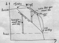
There is a good post by Dimitri, about first pole and second pole.
http://www.diyaudio.com/forums/showthread.php?postid=128238#post128238
a=emitor degeneration in VAS
b=miller compensation C-B in VAS
c=resistor between C-B in VAS
He said that second pole is
I calculate, with addition of Miller cap, the second pole time constant is bigger (ie=lower frequency), but why he wrote :
With miller cap around VAS, the "(C associated with VAS output node) is decreasing or increasing? What am I missing?
I try to understand what this base stopper do in the scope of the whole amp stability.
There is a good post by Dimitri, about first pole and second pole.
http://www.diyaudio.com/forums/showthread.php?postid=128238#post128238
a=emitor degeneration in VAS
b=miller compensation C-B in VAS
c=resistor between C-B in VAS
Dear capslock,
first pole time constant is (VAS input resistance)*(Cbc VAS)*(VAS gain)
second pole time constant is (output stage input resistance)*(C associated with VAS output node)
in your cases a) and c) the second pole time constant will remain unchanged and you should make much higher first pole time constant to move second pole below unity loop gain. Only in case b) you will get the second pole time constant lower (then original one) due to NFB via Miller capacitor. With higher frequency second pole you can use not so low the dominant one.
another nonlinearity is associated with VAS output node - nonlinear input current of the output stage. To makes this nonlinearity lower you should keep VAS output resistance low - again by Miller compensation. Here the advantage over c) will be that the VAS output resistance will be lower with frequency, that helps to keep associated disto at low level (please keep in mind that the overall loop gain is lower with frequency)
so for the discussed topology LTP-VAS-output stage b) is superior
He said that second pole is
second pole time constant is (output stage input resistance)*(C associated with VAS output node)
I calculate, with addition of Miller cap, the second pole time constant is bigger (ie=lower frequency), but why he wrote :
Only in case b) you will get the second pole time constant lower (then original one) due to NFB via Miller capacitor.
With miller cap around VAS, the "(C associated with VAS output node) is decreasing or increasing? What am I missing?
Attachments
mikeks :
Concerning optimum base drive for bipolar transistors, read that thread: http://www.diyaudio.com/forums/showthread.php?s=&threadid=60969
Concerning optimum base drive for bipolar transistors, read that thread: http://www.diyaudio.com/forums/showthread.php?s=&threadid=60969
Hi, EVA,
You make 0-15V DC supply, 120A, powered from 220VAC mains? That small? Incredible
One 0-15V DC supply, 100A that I know is ORION PS100, it weighs like hell
In that thread so many complex words. In what part the perfect bipolar drive is? I think I saw "Bipolar Drive Cell", but it is for switching. Can it be applied to analog audio devices?
Hi, Carlos,
Is that EVA's toroid on your avatar?
mikeks & lumanuaw:
Check post 35, third oscilloscope capture... (base current vs. collector current). Quick turn-off is achieved by progressively *drawing* up to 6 amps from the base of a NPN device whose Ic is 11A, and even in these circumstances, the device takes more tan one microsecond to start turning off while that current (charge) is being drawn (removed) from the BE junction. The picture also shows the charge storage process (6A sourced to the base for 1uS). This base current waveform looks much like the gate current waveform of a switching MOSFET (plus 2A continuously sourced due to beta).
How to apply these principles to audio amplifiers? I don't know any perfect approach, but I think that it's quite useful to know bipolar transistor behaviour at high frequencies. I hope that the purpose of B-E paralell resistors is clear now.
Carlos: Please stop using my pictures.
lumanauw said:Hi, Harry,
I'm not sure you can say something like : that it is the output stage that oscilates, because if you disconnect the output stage, the rest of the cct becomes stable.
Disconnecting output stage (that makes the rest of the cct stable) is not indicating at all that it is the output stage that oscilates. The front sections maybe stable, the output stage maybe stable, but when you join these 2, the whole thing becomes unstable, because you have Feedback. Joining 2 stable sections will be the same stable, if you don't have feedback between those 2.
Good point. You are right - the output stage could affect loop phase margin, even if it isn't in the loop, by the loading of the VAS.
lumanauw said:I'm confused. In Doug Self book, he said that "the total VAS collector impedance, a typical real value being 22Kohm"
Is the "total collector impedance" of VAS is the same as "output impedance" of VAS? VAS gives output from collector.
How can I understand the concept of "low impedance" and "high impedance" in the VAS output? Any" easy to understand" illustration here?
...
How to see the VAS in this "impedance" mode? It cannot gives the same voltage into any load, since the CCS that feeds VAS maybe only 4mA-10mA for example. If the load after the VAS demands current above 10mA, wouldn't this makes the VAS a "high impedance" output, since VAS cannot maintain it's output voltage into too demanding load?
lumanauw said:2. Is it true that VAS output is "low impedance output"? EVA's explenation that output impedance of VAS is inversely proportional to frequency indicates that in audio frequencies it is "high impedance" not "low impedance", towards the base of predrivers. The base of predriver has input impedance also inverse of frequency.
How to see this matter with "easy to understand" method?
When we talk about VAS impedance, we are talking about "AC small signal" or "incremental" impedance. The issue of a load demanding more than the VAS standing current is seperate - this will result in clipping (and before that, severe non-linearity), the value of the standing current does not result in a high impedance in the way which you suggest. The circuit should be designed so that the VAS doesn't get anywhere near being starved of current by the following stage.
In order to understand the collector impedance consider imposing a small AC voltage variation at the collector of the VAS transistor. What change in VAS current will this cause? If the transistor is operating in its linear region, a change of Vce should result in only a very small change in collector current, so the impedance 'seen' at the collector is high (small voltage change/much smaller current change = high impedance). At low frequencies this impdance should be equal to 1/the gradient of the tanget of the Ic Vs Vce curve of the transistor at the particular quiescent Vbe and Ic in question. Assuming the VAS is current-source loaded, the AC signals will 'see' this collector impedance in parrallel with the current source output impedance. As the current source output impedance is very high (a few Megohms), the collector impedance will dominate.
The above paragraph is assuming a low-frequency analysis. As the small-signal AC frequency is increased, the impedance seen at the collector will decrease, as explained by Eva. Also, note that in a stage with miller compensation, the VAS output impedance is significantly affected in audio frequency range by the feedback capacitor.
Eva said:By the way, what happens if base stopper resistors are removed? and what happens when they are placed between the VAS and the drivers instead?
I don't really want to remove the base stoppers completely. They are there more to ensure proper current sharing between the output devices rather than to try and stop oscillations. I could try reducing their value. Definitely the first thing I am going to try is reducing the resistance values in the feed-back path.
Eva said:mikeks :
Concerning optimum base drive for bipolar transistors, read that thread: http://www.diyaudio.com/forums/showthread.php?s=&threadid=60969
Good work Eva....cheers.
Eva said:Carlos: Please stop using my pictures.
Careful Carlos!!
She got my a.s.s. binned for weeks just for trying to chat her up!

I calculate, with addition of Miller cap, the second pole time constant is bigger (ie=lower frequency),
sorry, pal this is wrong, the second pole time constant would be lower (higher frequency). Read Solomon paper - Op amp - tutorial study
ece.wpi.edu/~mcneill/handouts/solomon.pdf
- Status
- This old topic is closed. If you want to reopen this topic, contact a moderator using the "Report Post" button.
- Home
- Amplifiers
- Solid State
- Base Stoppers