I'm not an expert but when you are talking about solely analog signals I don't think the side of the PCB makes much difference when you are using ground planes as all you are doing is moving the trace vertically by 1-2mm (the thickness of the PCB).
You can use the mirror button in Eagle to move components and traces to the other side of the PCB")
You can use the mirror button in Eagle to move components and traces to the other side of the PCB
Hi,
another question for the experts here.
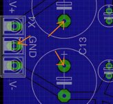
My main signal traces or better the majority of them are on the top surface where the components are located. My bottom layer has only a few, maybe 5 signal traces.
What do u-all think, should i swap them, e.g. put the majority of the traces on the bottom side?
Does this have any advantages, e.g. like less interfernce with the components?
If that's the case, is there an easy way to swap them with eagle w/o having lay them out again on the bottom layer?
Thanx Again,
Chris
I don't think it matters until you are laying out boards with signals in the tens or hundreds of megahertz.
Thanx again guys...
I did end up swapping the traces with eagles change tool. It will make the comp silk easier to read and it was my original intention to have the main traces on the bottom.
With eagle, one can reassign the layers quite easily. You have to make sure you get them all, else via's will be added! I also had to delete the ground planes and recreate them. Maybe there's an easier way to do that but it seemed to work. Afterwards, i did the obligatory electrical/design errors check. Everything seem's to be in order.
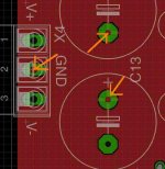
For the component grounding connections:
i guess the blue or red show's up depending upon which layer is active.
Guess both ground planes are connected, which seems logical, since both have the name "GND".
Blue = Bottom layer
Red = Top layer
See pics. I hope its ok. Never noticed this before, since I wasn't sensitive to it till now.
Cheers,
Chris
I did end up swapping the traces with eagles change tool. It will make the comp silk easier to read and it was my original intention to have the main traces on the bottom.
With eagle, one can reassign the layers quite easily. You have to make sure you get them all, else via's will be added! I also had to delete the ground planes and recreate them. Maybe there's an easier way to do that but it seemed to work. Afterwards, i did the obligatory electrical/design errors check. Everything seem's to be in order.
For the component grounding connections:
i guess the blue or red show's up depending upon which layer is active.
Guess both ground planes are connected, which seems logical, since both have the name "GND".
Blue = Bottom layer
Red = Top layer
See pics. I hope its ok. Never noticed this before, since I wasn't sensitive to it till now.
Cheers,
Chris
Attachments
Hi AndrewT,
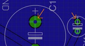
actually i think what u mean is something called "thermals" in eagle terminology.
These are little islands or circles around the component terminals that are place on the ground planes per default eagle setting.
They should make soldering to the ground plane easier, i hope.
Is this what u mean?
actually i think what u mean is something called "thermals" in eagle terminology.
These are little islands or circles around the component terminals that are place on the ground planes per default eagle setting.
They should make soldering to the ground plane easier, i hope.
Is this what u mean?
Attachments
I made a trial gerber run and viewed it.
It looks like it thinks my board dimension is larger than what i intended it to be. See orange outline in pic.
Is this really the physical board dimension?
In eagle i get something like 4.05 x 2.60, e.g. lower left edge of board is 0,0 upper right is 4.05,2.60.
Looks like my gerber file or viewer is including the regulator symbols into the board area.
Is this defined in some tDimension layer or something in gerber or eagle?
Do i just edit that in gerber, e.g. in the dimension layer?
Or can i do it in eagle, e.g. smash part or something?
I was assuming that the regulator symbols would be part of the silk screen which i could edit in gerber...
Cheers,
Chris
Attachments
There is board dimensions in eagle, its a white box that goes around your design. Is that what the orange box is?
Each component has a value and name, I think they are t_value and t_name or something. You can smash components and delete them if you don't want them. Or you can just not include those layers in the gerbers.
Each component has a value and name, I think they are t_value and t_name or something. You can smash components and delete them if you don't want them. Or you can just not include those layers in the gerbers.
Hi maxw,
no the orange box i painted in the snapshot but that's about how gerber is viewing it.
The problem is coming from the regulator mounting holes. They are included and that's why it thinks the board is bigger.
Actually the regulators will be upright but that's how eagle draws the symbol. Maybe i can tweak it in eagle somehow to make them "vertical".
Regards,
Chris
Hi me again....
I fixed the board area issue by changing the regulators to some verticals ones.
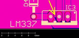
Here's a snapshot of the gerber results. I'm curious what some of you might about the spacing between the thick trace below the regulator. Is the spacing there too small. It doesn't appear to be less than the spacing between the traces and ground plane. The lowest horz. blue space is about 0.166 mm high.
I ran a board houses DRU file w/o errors.
Thanx for looking at it.
Chris
I fixed the board area issue by changing the regulators to some verticals ones.
Here's a snapshot of the gerber results. I'm curious what some of you might about the spacing between the thick trace below the regulator. Is the spacing there too small. It doesn't appear to be less than the spacing between the traces and ground plane. The lowest horz. blue space is about 0.166 mm high.
I ran a board houses DRU file w/o errors.
Thanx for looking at it.
Chris
Attachments
Hi me again....
I fixed the board area issue by changing the regulators to some verticals ones.
Here's a snapshot of the gerber results. I'm curious what some of you might about the spacing between the thick trace below the regulator. Is the spacing there too small. It doesn't appear to be less than the spacing between the traces and ground plane. The lowest horz. blue space is about 0.166 mm high.
I ran a board houses DRU file w/o errors.
Thanx for looking at it.
Chris
Just take care when you solder it so that you do not get a solder bridge.
0.166mm is very, very small (about 0.006"). It may pass DRU, but generally, such tight keep-away distances are reserved for high density digital boards with surface mount and ball grid arrays where sneaking traces between pins is an absolute necessity.
Also, board houses do make mistakes and I have seen occasional open traces, shorts, and bad vias. I have some recent boards where they simply missed one trace altogether.
Hello,
I've built a very similar circuit adapted from Chris2's final design although I used an NE5532 instead of an OPA134.
I was having an issue with DC on the output of the NE5532 so replaced the 68R resistor with a 47uF cap and a 22K DC drain resistor.
The problem I've noticed is that there is a difference of between 20mA - 50mA (I built serveral circuits) on the + & - output of the DRV134. Any idea what may be causing this?

Last edited:
- Status
- This old topic is closed. If you want to reopen this topic, contact a moderator using the "Report Post" button.
- Home
- Source & Line
- Analog Line Level
- Balanced Line Driver with DRV134