Not forgotten about. I am still uncertain we have come to a good conclusion of a design.
How about a pole?
RodeoDave has done lots of work on this, and I like elements of Prooptiki's design as well. If a consensus is not drawn, and some other question remain unanswered, I will decide on something. We need to make sure we are not bothering anyone's intellectual property.
Regards,
Tea
... of course I do not know which is the better solution.
About intellectual property, do you think we should ask directly to Nelson Pass?
Regards
")
I still owe y'all the layout I worked out for my build, I'll try to post it soon.
Another question that maybe needs to be discussed is whether or not we want to use the kind of hard to get 2SK170BL jfets...
Which are others candidates? Does the layout change with different jets?
Any news ?
I still owe y'all the layout I worked out for my build, I'll try to post it soon.
Another question that maybe needs to be discussed is whether or not we want to use the kind of hard to get 2SK170BL jfets...
Yes and no.
I discussed with Nelson about current proposed schematics, none appear to rip of his work, and he admits his work is not totally original (but cleverly implemented).
The next issue will be to make the design to keep it fairly absent of direct use of Salas DCB1 buffer. Hence, if you want a buffered output, it needs to go back into a DCB1 board. Make use of the power supply to power buffer and x-over, and then load the signal from the x-over.
Once that is ironed out, we look at Dave's layout, and Prooptiki's layout - assume they follow those rules and discuss the solution from there. I of course will make the final decision if I am going to prototype the boards in a factory. Linear systems also offers LSK170B that will fit the bill of parts if one wants to conform to that. Of course this assumes that there is liberal use in IDSS ranges that can be used in the design.
I am about to start a P2P version of this on perf board. Tired of waiting for a pcb. Once I get it wired, I'll post a pic or two.
In terms of matching jFETs, I assume only each pair need to be matched, correct? If not a perfect match, which should be the higher IDS? Top (V+ side) or bottom (V-)
In terms of matching jFETs, I assume only each pair need to be matched, correct? If not a perfect match, which should be the higher IDS? Top (V+ side) or bottom (V-)
the high pass has a capacitor as it's input. This very effectively blocks DC from a previous stage. As such the high pass jFETs do not need to be selected for ultra low output offset. 1mVdc or 2mVdc from each stage does not matter.
The low pass does not have a DC blocking cap at it's input. Here successive stages will accumulate offsets. But you can easily block these offsets with a final coupling cap or even with intermediate coupling caps. At the typical input impedance of around 5K to 20k, each Low pass stage would need a fairly large coupling cap to preserve the LF.
I would (I did) adopt the single ended version and use input and output coupling caps.
Rough selection of jFETs gives me very acceptable stage voltages.
No matching required.
I did use B or bl with 2r2 source resistors in the CCS half. This reduces dissipation slightly but also ensures no jFET operates with >Idss and thus avoids the gate leakage risk if they get too hot.
Last edited:
the high pass has a capacitor as it's input. This very effectively blocks DC from a previous stage. As such the high pass jFETs do not need to be selected for ultra low output offset. 1mVdc or 2mVdc from each stage does not matter.
That makes sense.
OK, so the problem with mismatched jFETs is that you can get DC offset and this could accumulate in successive stages, correct? How closely do they need to be matched to avoid problems? Since I will be working with 48 jFETs and only half of them need to be matched, it would seem likely I could get pretty good matching.The low pass does not have a DC blocking cap at it's input. Here successive stages will accumulate offsets. But you can easily block these offsets with a final coupling cap or even with intermediate coupling caps. At the typical input impedance of around 5K to 20k, each Low pass stage would need a fairly large coupling cap to preserve the LF..
So the B1 had a 1uF cap before the jFETs and a 10uF after it. Would a 1uF before the first stage (the buffer before you split the signal to Hi pass, Low pass) and then a 10uF at the end of the Low pass be sufficient? Or would you need 1uF before each stage? Wouldn't the cap upset the LR4 frequency if used other than at the input buffer and after the final stage?I would (I did) adopt the single ended version and use input and output coupling caps.
Rough selection of jFETs gives me very acceptable stage voltages.
No matching required..
Does this 2r2 go between the V- and the Source of the "bottom" (CCS) jFET? Or between the Gate and Source? I don't follow its operation. Also, assuming I do match as closely as possible (How close is close?) is this necessary? If there is any mismatch (.01, .001?) does the higher IDSS go on the top or bottom?I did use B or bl with 2r2 source resistors in the CCS half. This reduces dissipation slightly but also ensures no jFET operates with >Idss and thus avoids the gate leakage risk if they get too hot.
Thanks for helping me understand this better.
You don't need matched jFETs.
Just select similar Idss.
When the upper and lower run at Idss the output offset is ZEROmV.
When the upper runs at something other than Idss, then that results in an output offset.
If the CCS is set to pass less than the Idss of the upper, then that too results in an output offset.
For a typical 7mA to 9mA Idss, I would estimate that 0.1mA variation is perfectly acceptable and even 0.2mA is probably OK, provided you DON'T ask the upper device to pass more than Idss.
If you use a single ended version, then accumulation of 5mV offset per stage consisting of Input Buffer + 2pole LP + 2pole LP + Output Buffer adds up to only 20mV of total offset from the ideal midway bias. But even midway bias is not ideal since these source followers develop significant 2nd harmonic when output nears the supply rails.
That's why we use signal around 2Vac in a +-10Vdc ( or +20Vdc) supply. The 10dB to 11dB headroom between maximum signal level and stage clipping level is used so that the 2nd harmonic stays very low.
Read Dennis Feucht.
His paper on biasing jFETs is very instructive.
If you use his circuit and set the two Source resistors to 0r0, you get the Pass B1 circuit.
Attachments
Last edited:
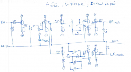
Here's something I sketched up during lunch break. Buffered passive BSC in front of 2nd order (12dB/octave) HP/LP and relative level control for HP.
Should be managable to fit this on half a eurocard. Unfortunately I'm not familiar with pcb design software. What are you guys using?
I'm not sure if a pcb version can be reasonably kept fairly absent of direct use of Salas DCB1 buffer. What's the verdict?
Should be managable to fit this on half a eurocard. Unfortunately I'm not familiar with pcb design software. What are you guys using?
I'm not sure if a pcb version can be reasonably kept fairly absent of direct use of Salas DCB1 buffer. What's the verdict?
Attachments
Here's something I sketched up during lunch break. Buffered passive BSC in front of 2nd order (12dB/octave) HP/LP and relative level control for HP.
Should be managable to fit this on half a eurocard. Unfortunately I'm not familiar with pcb design software. What are you guys using?
I'm not sure if a pcb version can be reasonably kept fairly absent of direct use of Salas DCB1 buffer. What's the verdict?
Thanks Dave,
For previous suggested incarnations we have Nelsons permission to move forward.
If we want to use Salas design within the card itself, we have to discuss with Salas his IP on the matter, and compensate him for using it preferably. Using a DCB1 as a power source and output buffer would seem to simplify things. Those boards are readily available with his blessing and support. I am not sure in this design how close or what it barrows from his design.
This has generated enough interest that I think it makes sense to start a separate thread, so here it is. If the moderators could move the relevant posts from the B1 Buffer Preamp thread to here it would be much appreciated.
A solution to the bandstop response issue in the low pass section is to provide a separate buffer for the feedback cap, blocking the forward signal path to the output. This increases the stopband attenuation to greater than 100 dB.
I've eliminated the trimpot from the LP section, as I don't need it in my particular application.
I've been busy with work, but I'll post more here as soon as I get an opportunity.
Cheers,
WOW thanks Jacques Merde
after suffer few days from this stopband i found your scheme with help from AndrewT

I'd still like to see the pcb happen.
I'm currently reevaluating the configuration of the XO. What's you guys' opinion on the following:
That way we should end up with better S/N ratio, no? And since tweeters (or midrange in 3 way systems) are generally more sensitive than woofers, only the HP branch needs a relative level control, no?
I'm currently reevaluating the configuration of the XO. What's you guys' opinion on the following:
- BSC followed by another buffer AFTER the low pass
- Output level control followed by another buffer AFTER the high pass
That way we should end up with better S/N ratio, no? And since tweeters (or midrange in 3 way systems) are generally more sensitive than woofers, only the HP branch needs a relative level control, no?
A big !thank you! goes out to the Master Nelson Pass...
We can add a third way, plus Notch filter, plus Delay correction... with some help with opamps or a discrete opamp...
Small changes, for discussion .... from post 395 : http://www.diyaudio.com/forums/pass-labs/156094-b1-active-crossover-40.html#post4272065
Need some help to offer choices of shelving equalization curve, for now only 1khz.
We can add a third way, plus Notch filter, plus Delay correction... with some help with opamps or a discrete opamp...
Attachments
Last edited:
- Status
- This old topic is closed. If you want to reopen this topic, contact a moderator using the "Report Post" button.
- Home
- Amplifiers
- Pass Labs
- B1 Active Crossover