optimum capacitor ratio
Unpublished papers don't count. Besides, you contradict yourself:
(From the "Bob Cordell Interview: Negative Feedback" thread, 28th December 2010)
Actually I first pointed this out in a paper I wrote back in 2004, as Jan Didden can confirm-many years before Harry Dymond's AES paper was published.
[...]
Unpublished papers don't count. Besides, you contradict yourself:
There is no such thing as an optimum ratio. The only requirement is that the series combination of C1 and C2 should equal the value of the capacitor you would use for single pole compensation.
(From the "Bob Cordell Interview: Negative Feedback" thread, 28th December 2010)
Indeed, it can work.
But first, read this about the optimal capacitor ratio for TPC.
It is Harry Dymond who deserves all the credits for pointing this out.
Next, look here how TPC + TMC should not be implemented.
And finally look here for one of the correct possible implementations.
Bottom line: all these Nth order compensation schemes only make sense if the stage (i.e. the TIS) to which it is applied, has sufficient gain.
Also notice the shunt compensation (C8 & R21) Do you hear me Mr Self? I repeat SHUNT compensation. Also Bob Cordell calls this shunt compensation.
Cheers,
E.
Hi Edmond,
I have read all those before, but my simulation shows different result. When I swap C5 with C23 THD20k jumps from 0.000020% to 0.000071% with all else kept the same. I could be that my values are not optimal but still way I’ve got that result?
BR Damir
Attachments
Hi Waly,
The ThermalTraks are surely not perfect devices, and many approaches to using them have failed. Moreover, there necssarily is some tweaking of the relative temperature compensation of the drives and the output devices for any given amplifier with any given approach to heatsinking (for example, how are the drivers heatsinked? Are they on the main heatsink or do they have their own? Where are the pre-drivers heatsinked in the case of a Triple? As mentioned in my book, I try to use bias spreader circuits that allow for some thermal feedback from the driver and the output stage to allow establishing the best balance. I'll be the first to admit that it takes some experimentation on the specific amplifier, but I have been able to achieve very good results, as shown by some of the figures in my book. Their faster response to the actual conditions on the power transistor die is very helpful. Nevertheless, they are certainly not perfect.
The output stage bias is important, and I have always been troubled by the way it moves all over the place with traditional approaches to bias temperature compensation.
Until ThermalTraks came along, I was much more comforatble with power MOSFETs in this regard. Not only are they less fussy about bias, since with them the more the better, but they are at the end of the day less variable in bias with changing conditions of warm-up and program material.
Cheers,
Bob
Hi Bob,
I bought your book before I finished my TT amp, and I used your suggestion for bias spreader. What I noticed is that I need to readjust some resistors in the bias spreader from amp to amp to make it functions as intended. It looks that there are differences between some of diodes integrated in TT transistors. After some adjustment the bias current was stable and amp worked very good, now more a year in service. I bought my TT transistors a long time ago (don’t remember the year) could be the first production. Did you have similar problem?
I mounted the bias spreader on separate heat sink with the driver on it.
BR Damir
Hi Damir,
When I swap C1 and C2 in my schematic, I also get lower distortion. BUT... at the same time the ULGF gets higher (which explains the lower distortion) and the phase margin gets lower. IOW, it's a trade-off between stability and lowest distortion.
Cheers,
E.
When I swap C1 and C2 in my schematic, I also get lower distortion. BUT... at the same time the ULGF gets higher (which explains the lower distortion) and the phase margin gets lower. IOW, it's a trade-off between stability and lowest distortion.
Cheers,
E.
Last edited:
Hi Damir,
When I swap C1 and C2 in my schematic, I also get lower distortion. BUT... at the same time the ULGF gets higher (which explains the lower distortion) and the phase margin gets lower. IOW, it's a trade-off between stability and lowest distortion.
Cheers,
E.
Hi Edmond,
In my case the ULGF vent from 2.03MHz to 2.35MHz and the phase margin stayed the same(55 degree), but distortion dropped by 11dB. For me that swapping worked, stability did not suffer.
BR Damir
It is not a very good idea to have drivers on the main heatsink. Some makers of renowned
amps proverbially swear on separate heatsinks for each device. In order to achieve this PCB layout can be a cumbersome task. Rarely mentioned is to keep high current stage off the PCB.
amps proverbially swear on separate heatsinks for each device. In order to achieve this PCB layout can be a cumbersome task. Rarely mentioned is to keep high current stage off the PCB.
Well, I have the pre- drivers and the drivers on the main Heatsinks and I have no problems with stability.
I think there is a tendency to make a mountain out of a molehill on this issue. EF2's I find are easy to thermally compensate, but EF3 is a lot tougher.
I am afraid fast (ms) response times to changes in output stage dissipation are not going to be possible without on-chip sensing on all 3 of the output devices in 1 half of a triple and a lot of peripheral circuitry. Will you hear the difference? No.
Further, although the TT devices sense diode is not tightly matched with the output device dVbe, you can adjust the slope somewhat by adjusting the diode current.
Last edited:
Hi Bob,
I bought your book before I finished my TT amp, and I used your suggestion for bias spreader. What I noticed is that I need to readjust some resistors in the bias spreader from amp to amp to make it functions as intended. It looks that there are differences between some of diodes integrated in TT transistors. After some adjustment the bias current was stable and amp worked very good, now more a year in service. I bought my TT transistors a long time ago (don’t remember the year) could be the first production. Did you have similar problem?
I mounted the bias spreader on separate heat sink with the driver on it.
BR Damir
Hi Damir,
I take it to mean that you have to adjust some resistors in the bias spreader from amp to amp of the identical design and implementation, both electrical and physical. I also take it that these adjustments are not just for establishment of the nominal bias current, but rather for the long-term thermal stability as a function of time. If both of these are true, then it is indeed strange.
I have not seen significant differences in the ThermalTrak diode among different ThermalTrak transistors, but my sample size was not large. It is conceivable that they used some different diodes, but that seems unlikely apart from batch-batch diode variations of the same diode type. Also, I think it would have to be a substantially different diode to cause the needed adjustment you describe, again if I understand what you are describing.
Cheers,
Bob
It is not a very good idea to have drivers on the main heatsink. Some makers of renowned
amps proverbially swear on separate heatsinks for each device. In order to achieve this PCB layout can be a cumbersome task. Rarely mentioned is to keep high current stage off the PCB.
I usually prefer separate heatsinks for the drivers and predrivers, as their thermal behavior is different, for one thing (the drivers and pre-drivers have a fairly constant power dissipation as a function of program material).
In one of my ThermalTrak designs, I place a 1/8 inch aluminum bar across the circuit board and mount all of the drivers and predrivers on it, as well and a thermal sense transistor that is part of a Vbe multiplier that is there specifically for those transistors. That whole group of transistors is isothermal to first order. I then also have the ThermalTrak transistor diodes incorporated into that Vbe multiplier to compensate for the output stage device temperatures. This is similar to Figure 14.19 in "Designing Audio Power Amplifiers".
However, I have done designs where the drivers were on the heatsink as a matter of convenience because the drivers do dissipate a modest amount of power, and it is easier to get rid of it on the main heatsink. These designs can be made to work with good thermal stability as well.
Cheers,
Bob
Hi Damir,
I take it to mean that you have to adjust some resistors in the bias spreader from amp to amp of the identical design and implementation, both electrical and physical. I also take it that these adjustments are not just for establishment of the nominal bias current, but rather for the long-term thermal stability as a function of time. If both of these are true, then it is indeed strange.
I have not seen significant differences in the ThermalTrak diode among different ThermalTrak transistors, but my sample size was not large. It is conceivable that they used some different diodes, but that seems unlikely apart from batch-batch diode variations of the same diode type. Also, I think it would have to be a substantially different diode to cause the needed adjustment you describe, again if I understand what you are describing.
Cheers,
Bob
Hi Bob,
My first TT amp was made with NJL3281/1302 transistors and those were from old production, I ordered them soon after they vent into production, and I have had diode problem with them. I use the bias spreader from your book Figure 14.19 and I needed to change R1, in one channel I used 1200 ohm in other 1500 ohm to get long term bias current stability. Actually I noticed different voltage drop on some of the TT diodes.
I have NJL0282/0302 and NJL4281/4302 also, but not yet tested. They are ready for that(PCB is populated) and I hope there is not going to be the same problem.
Thanks for your comment.
BR Damir
I have NJL0282/0302 and NJL4281/4302 also, but not yet tested. They are ready for that(PCB is populated) and I hope there is not going to be the same problem.
Hi Damir.
I have rails of NJL4281/4302 too.
A while back there was information that the diode is different from the other NJL transistors.
The difference was sufficient that some thermal bias circuits required modification.
I hope you have noticed this already, or that your circuit is more adaptable than mine.
What circuit is on your PCB?
Best wishes
David
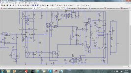
Also notice the shunt compensation (C8 & R21)
Hi Edmond
Did you consider to move C8 and R21 so they are a nested Miller compensation just around the VAS/TIS?
That is, back to the base of Q6 rather than earth, and smaller capacitance.
Best wishes
David.
Hi Damir.
I have rails of NJL4281/4302 too.
A while back there was information that the diode is different from the other NJL transistors.
The difference was sufficient that some thermal bias circuits required modification.
I hope you have noticed this already, or that your circuit is more adaptable than mine.
What circuit is on your PCB?
Best wishes
David
Hi David,
As I said I did not try NJL4281/4302 yet only NJL3281/1302. My amp is the same as here in this asc file but with TMC only:http://www.diyaudio.com/forums/soli...-self-wants-your-opinions-51.html#post3444174
BR Damir
And I am VERY disappointed that the basic idea of a long-tailed pair is not clear to you.???
I'm VERY disappointed to read this under the Douglas Self signature
No. In the LTP the second-harmonic distortion is is cancelleled. This is easily demonstrated mathematiclaly, by simulation, and measurement.Any distortions added to the output signal before it is substracted will add distortion.
Yes, but utterly wrong.Am-i clear ?
Apologies for taking so long to reply, but I have been designing amplifiers. With LTPs.
I usually prefer separate heatsinks for the drivers and predrivers, as their thermal behavior is different, for one thing (the drivers and pre-drivers have a fairly constant power dissipation as a function of program material).
Cheers,
Bob
Physics is somewhat helpful here. It can be shown that placing each and every device on separate heatsinks has two advantages over a main heatsink.
First: a larger heatsink has higher thermal capacity but the value of its thermal resistance refers to a constant surface temperature thus that the temperature gradient is zero. This is hardly ever the case thus one has a temperature gradient and usually the place where the dissipative device is mounted is the hottest.
Thus dynamically the thermal resistance seen from the dissipative junction
is higher than the specified thermal resistance.
Second: no electrical insulating of the device and the heatsink is necessary.
That saves around 1°K/w thermal resistance thus the individual heatsink becomes smaller and - dynamically - "faster".
And further no however small capacitance collector to ground is added.
Oh yes I can.Now, about this old sea snake CFA vs VFA.
So, Doug, i understand you can be afraid to enter in this very controversial VFA vs CFA subject (i don't know why it is-it), but you cannot deliberately forget to talk about CFAs in your book,
But you are quite wrong. The use of a single transistor as opposed to an LTP in the input stage does not make it what is commonly called a CFA. There is also the VAS operation to be considered.After all, what we call a current feedback configuration is just to use the same input active device in two different way: common emitor for the signal, common base (which is fast) for the feedback.
I hope you've not been tampering with any of the desks I designed.I will just add that, in all analog mixing desks i had modified, there is a great improvement, in the mixing bus input stages, to swap to current feed-back OPAs.
Hi Damir,
first I want to agree: superb performance for this "rather simple" topology. Difficult not to be thrilled.
The loop behaviour around 50 Khz (almost positive feedback) is, as I understood quite late , of course due to the two-pole compensation with its slope of 40 dB per decade.
I played a little bit with your schematics. Being always conservative, I was interested in the VAS stability under TPC conditions. For that (bode-VAS.png), I shorted the main NFB loop by C27 at the negative LTP input and turned off your AC source V6. Then I added a new source V7 in the loop around the VAS. What I did not know to cope with was the TMC connection via R30. For simplicity, I just made it almost isolating.
The outcome is in bode-VAS-result.png.
The phase margin is around 30 degrees. Do not know whether this is already critical. At least does the KSA992 model include a base spreading resistance RB, so it might be realistic.
My general question is: how can one cleanly evaluate the behaviour of the three intertwinned feedback loops i) main loop ii) loop around VAS iii) loop around OPS/VAS due to TMC? Did you already reason about that?
Would be a pity if one could only observe e.g. the transient response on a square wave and hope that everything is nice if that looks OK.
Greetings,
Matze


first I want to agree: superb performance for this "rather simple" topology. Difficult not to be thrilled.
The loop behaviour around 50 Khz (almost positive feedback) is, as I understood quite late
, of course due to the two-pole compensation with its slope of 40 dB per decade.I played a little bit with your schematics. Being always conservative, I was interested in the VAS stability under TPC conditions. For that (bode-VAS.png), I shorted the main NFB loop by C27 at the negative LTP input and turned off your AC source V6. Then I added a new source V7 in the loop around the VAS. What I did not know to cope with was the TMC connection via R30. For simplicity, I just made it almost isolating.
The outcome is in bode-VAS-result.png.
The phase margin is around 30 degrees. Do not know whether this is already critical. At least does the KSA992 model include a base spreading resistance RB, so it might be realistic.
My general question is: how can one cleanly evaluate the behaviour of the three intertwinned feedback loops i) main loop ii) loop around VAS iii) loop around OPS/VAS due to TMC? Did you already reason about that?
Would be a pity if one could only observe e.g. the transient response on a square wave and hope that everything is nice if that looks OK.
Greetings,
Matze
Capacitive load
Hi Damir,
here is also the main loop's Bode diagram for purely capacitive loads (green 1pf, yellow 10nF, red 20 nF). The load resistor is 1Kohm.
With no-nonsense speaker cables such capacities clearly should be out of reach, but High-End audiophile cables can reach these values.
Cheers,
Matze

Hi Damir,
here is also the main loop's Bode diagram for purely capacitive loads (green 1pf, yellow 10nF, red 20 nF). The load resistor is 1Kohm.
With no-nonsense speaker cables such capacities clearly should be out of reach, but High-End audiophile cables can reach these values.
Cheers,
Matze
in the Cordell Book thread I showed several ways to test loop gain that give a fairly accurate result for TMC - you have to measure inside both loops enclosing the output Q
http://www.diyaudio.com/forums/soli...s-self-wants-your-opinions-8.html#post3402379
the square wave response for TMC doesn't indicate stablity margin as we are used to with simple dominant pole Miller compensated amps - a reason for warnings against using TMC if you don't understand stability evaluation at a pro EE level, would be "nervous" using 2-pole - they are similarly complcated, TMC easliy measured incorrectly
Hi Damir,
first I want to agree: superb performance for this "rather simple" topology. Difficult not to be thrilled.
The loop behaviour around 50 Khz (almost positive feedback) is, as I understood quite late
I played a little bit with your schematics. Being always conservative, I was interested in the VAS stability under TPC conditions. For that (bode-VAS.png), I shorted the main NFB loop by C27 at the negative LTP input and turned off your AC source V6. Then I added a new source V7 in the loop around the VAS. What I did not know to cope with was the TMC connection via R30. For simplicity, I just made it almost isolating.
The outcome is in bode-VAS-result.png.
The phase margin is around 30 degrees. Do not know whether this is already critical. At least does the KSA992 model include a base spreading resistance RB, so it might be realistic.
My general question is: how can one cleanly evaluate the behaviour of the three intertwinned feedback loops i) main loop ii) loop around VAS iii) loop around OPS/VAS due to TMC? Did you already reason about that?
Would be a pity if one could only observe e.g. the transient response on a square wave and hope that everything is nice if that looks OK.
Greetings,
Matze
View attachment 341324
View attachment 341325
I have simulated TPC for several times, but I have never tried one in real.
Why?
If you look at the square wave response, it seems that most TPC amplifiers are underdamping, it takes rather a long time to settle down. It's about 3 or 4 times longer than one pole system. A well turned 2 pole system should have a much better step response. Unless I find a good way to solve this issue, I won't put it in real.
- Status
- This old topic is closed. If you want to reopen this topic, contact a moderator using the "Report Post" button.
- Home
- Amplifiers
- Solid State
- Audio Power Amplifier Design book- Douglas Self wants your opinions