pet-240,
I meaned in fact: Cubitruck board : around 100 US dollars : awsome for the price an little : put it in your DAC to have an embeded muisc server, oversampling on the fly, movies server, what you like (thanks to Soundcheck fellow for the hint ! ) Cubieboard | A series of open source hardware
I meaned in fact: Cubitruck board : around 100 US dollars : awsome for the price an little : put it in your DAC to have an embeded muisc server, oversampling on the fly, movies server, what you like (thanks to Soundcheck fellow for the hint ! ) Cubieboard | A series of open source hardware
Thanks for the explanation, could you draw it out as per schematic?. mu=300?, triode?.. some tube.. whats the Rp?… and the type/number?
In the end, maybe we can compile all together a series of circuits to build and try.. productive and sharing. You have mine. Please share - and did you build the circuit?..
Shane
Hi Shane,
rp is the plate resistance. This is the measurement of plate voltage change over plate current change for a constant value of grid voltage. In other words, this is an expression of how much the tube acts like a resistor for any given amount of grid voltage. May be also determined by dividing the amplification factor by the transconductance: mu/gm. Its value remains constant along the linear portion of the tube characteristic.
For example, using a pair of 6C45P-E in the Broskie I to V (mu around 50, transconductance around 45mA/V, rp is around 1500 ohm), the theoretical minimum input impedance is 0.6 ohm (1500/(50*50)). In the real world the input impedance will result higher, maybe from 1.5 to 2 ohm using a strong bias for V1 tube such as 30mA or more.
Current output DACs loves to see a very low impedance, practically a virtual ground, so this approach could be very interesting. Moreover the tube I'm thinking to use as the V1 is very very linear, so the distortion should be very low.
The tube named THE_QUEEN has really mu from 250 to 300, this is a very special tube, a masterpiece of technology. Its gm is around 65000 uohms.
I have not yet built the circuit, I'm planning to build it in a couple of months.
Please, let me build and listen to, then I'll share all the information, the final circuit, the parts list, the power supply and finally the tube type.
I prefer to share all the information when the circuit will be built and it will work properly, as I shared all the info about my regulator when it was built and tested
http://www.diyaudio.com/forums/power-supplies/212476-well-regulated-power-supply-13.html
The only problem is that I have just a little free time to spend in diy, so my times are usually long.
For those who was interested, my scheduled jobs are:
- build and test my first version of the master clock. I got the PCB a week ago. After building and testing I'll open a new thread about master clock, and I could supply the PCB and the crystal
- building an SMD version of the regulator mentioned above (at this moment I'm designing the PCB)
- since the master clock needs two separate shunt regulators (+15V and +5V), I'm working on this power supply (still on the breadboard). Now I'm using a pair of Tentlabs shunt regulator
- finally the tube DAC I to V
Each time one project will be ready I will be glad to share my experience and supply some parts (eg. the PCB) when possible.
Stay tuned!
Andrea
Not aware myself about tubes designs but what about the Gomez than T. Loesch use in him C-77 flag ship ?
Studiostevus fellow has maybe an interresting experience : http://www.diyaudio.com/forums/digi...any-good-tda1541a-dac-kit-68.html#post3876062
too old design ? problem of cost or sourcing with some NOS tubes ?
Studiostevus fellow has maybe an interresting experience : http://www.diyaudio.com/forums/digi...any-good-tda1541a-dac-kit-68.html#post3876062
too old design ? problem of cost or sourcing with some NOS tubes ?
Hi Shane,
rp is the plate resistance. This is the measurement of plate voltage change over plate current change for a constant value of grid voltage. In other words, this is an expression of how much the tube acts like a resistor for any given amount of grid voltage. May be also determined by dividing the amplification factor by the transconductance: mu/gm. Its value remains constant along the linear portion of the tube characteristic.
For example, using a pair of 6C45P-E in the Broskie I to V (mu around 50, transconductance around 45mA/V, rp is around 1500 ohm), the theoretical minimum input impedance is 0.6 ohm (1500/(50*50)). In the real world the input impedance will result higher, maybe from 1.5 to 2 ohm using a strong bias for V1 tube such as 30mA or more.
Current output DACs loves to see a very low impedance, practically a virtual ground, so this approach could be very interesting. Moreover the tube I'm thinking to use as the V1 is very very linear, so the distortion should be very low.
The tube named THE_QUEEN has really mu from 250 to 300, this is a very special tube, a masterpiece of technology. Its gm is around 65000 uohms.
I have not yet built the circuit, I'm planning to build it in a couple of months.
Please, let me build and listen to, then I'll share all the information, the final circuit, the parts list, the power supply and finally the tube type.
I prefer to share all the information when the circuit will be built and it will work properly, as I shared all the info about my regulator when it was built and tested
http://www.diyaudio.com/forums/power-supplies/212476-well-regulated-power-supply-13.html
The only problem is that I have just a little free time to spend in diy, so my times are usually long.
For those who was interested, my scheduled jobs are:
- build and test my first version of the master clock. I got the PCB a week ago. After building and testing I'll open a new thread about master clock, and I could supply the PCB and the crystal
- building an SMD version of the regulator mentioned above (at this moment I'm designing the PCB)
- since the master clock needs two separate shunt regulators (+15V and +5V), I'm working on this power supply (still on the breadboard). Now I'm using a pair of Tentlabs shunt regulator
- finally the tube DAC I to V
Each time one project will be ready I will be glad to share my experience and supply some parts (eg. the PCB) when possible.
Stay tuned!
Andrea
Hi Andrea,
Thank you for the comprehensive reply, really appreciated.
With availability and pricing of such tubes becoming a concern, and with no real info that I can find about 'The Queen', appart from the british monarchy, can you link to a data sheet, or perhaps provide a number equivalent. I have a feeling its perhaps not so common.
With gain that high and practical limitations I would expect Rp to be almost pentode like.. maybe in this application it is not of concern as its coupled to a second stage, but perhaps it is.. depending on the Cin of that second tube and HF limitations (which may or may not be of benefit in this case with 1541A) I like the way grounded grid avoids miller effect, and look forward to learning more from your experiments..
Regards,
Shane
Hi Shane,
yes, I followed your advise and went for the the I2S to PCM from Ian for the silmutanous mode.
May you please go to the link I gave and explain to av-trouvaille fellow each Ian module in one phrase maxi (why one module with two clock, why one with one clock...)
It is a thrad for wookies, stay very simple in your explanation... If you have time for that of course !
Sure.. and thanks for the informations about the special cheeses from the Piedmont Region of Italy. I will be sure to search for the produce locally.
Shane
Have one, haven't found an os I like yet on it.
Nor have I found any oversampling I like.
Will read his article and see what he is using, thanks for the link!
Chuz,
Drew.
In the Cubietruck (cubieboard V 3) which arrive soon, they will allow a A80 processor : 8 G0 ram if you want...
Do you saw on the link, the cubieboard with the DAC stacked on it ? A squeezebox but with a fedora, a Debian or an Ubuntu OS ( I see no reason not to put in it a Seven also for the none linux specialists ) + a Foobar or Jriver and all the modules you want. Of course a minipc with no fan on second hand is enough...
With availability and pricing of such tubes becoming a concern, and with no real info that I can find about 'The Queen', appart from the british monarchy, can you link to a data sheet, or perhaps provide a number equivalent. I have a feeling its perhaps not so common.
Shane,
The Queen is not Elizabeth II, but a real triode.
The average characteristics are:
Amplification factor: 250 to 300
Transconductance: 50000 to 65000 microohms
Max plate voltage: 270V
Plate current: 33mA
Plate dissipation: 7.5W
Spice model:
.SUBCKT TheQueen 1 2 3; A G C;
* Extract V1.035
* Model created: 7-Feb-2014
+ PARAMS: MU=248.27 EX=1.476 KG1= 16.3
+ KP= 777.9 KVB=16656.
+ RGI=2000
+ CCG=11.2P CGP=1.45P CCP=0.019P ;
E1 7 0 VALUE=
+{V(1,3)/KP*LOG(1+EXP(KP*(1/MU+V(2,3)/SQRT(KVB+V(1,3)*V(1,3)))))}
RE1 7 0 1G
G1 1 3 VALUE={0.5*(PWR(V(7),EX)+PWRS(V(7),EX))/KG1}
RCP 1 3 1G ; TO AVOID FLOATING NODES IN MU-FOLLOWER
C1 2 3 {CCG} ; CATHODE-GRID
C2 2 1 {CGP} ; GRID-PLATE
C3 1 3 {CCP} ; CATHODE-PLATE
D3 5 3 DX ; FOR GRID CURRENT
R1 2 5 {RGI} ; FOR GRID CURRENT
.MODEL DX D(IS=1N RS=1 CJO=10PF TT=1N)
.ENDS
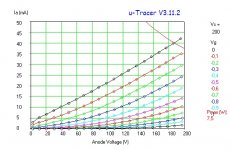
Attached you can find the the plot from the curve tracer.
Let me give a try, the I'll share all.
Andrea
Attachments
Andrea,
I know curves don't tell the whole story… but given that the increments are on order of 100mV - which is directly applicable to DAC output stage (1541A specifically), assume horizontal load line (as recommended by Broskie in his article that you linked to) - this tube does not seem very linear in its transfer function at all.
Also, is the scaling correct ?.. thats a massive change in plate voltage for a shift in such small grid voltage with plate current being held as a constant.
What is it that I am missing?
Shane
Last edited:
Andrea,
I know curves don't tell the whole story… but given that the increments are on order of 100mV - which is directly applicable to DAC output stage (1541A specifically), assume horizontal load line (as recommended by Broskie in his article that you linked to) - this tube does not seem very linear in its transfer function at all.
Also, is the scaling correct ?.. thats a massive change in plate voltage for a shift in such small grid voltage with plate current being held as a constant.
What is it that I am missing?
Shane
Shane,
this tube works usually biased with the grid around 0V, so the grid go positive during the signal swinging. In the circuit I posted the signal applied to the grid swings from -50 mV to +50 mV. Since the triode has a very high transconductance, the voltage swing to drive the tube to get great variation in plate current is very low, so the tube works anyway in its linear region (see the plot from 0V to -0.3V).
So the massive change in plate voltage for a shift in such small grid voltage is due to its high transconductance. If you set constant plate current, for small change in grid voltage you get great change in plate voltage.
Andrea
Hi guys,
Andrea, what is your wisch for the clock frequencies in your futur own needs ? 12.xx or 6.xx ?
I asked two questions to Ian about him I2S to PCM board : lake of uf.l connectors option for the inputs (links from the USB to I2S device). Which is strange as he allowed this option for the output. In fact I don't want the FIFO and the input connector does not match with any I2S to USB output connectors....
In relation to your clock board or any standalone clock board I asked some precision about the speed as well : http://www.diyaudio.com/forums/digi...rsal-i2s-pcm-driver-board-67.html#post3978542
Another thing is my try to understand the USB devices in relation to the Ian's IS to PCM board for the TDA1541 : http://www.diyaudio.com/forums/digi...erstanding-non-specialists-2.html#post3978518
Last edited:
btw, a good hint from Marce : http://www.diyaudio.com/forums/digital-line-level/258467-usb-spdif-recommendations.html#post3978066
the lower speed, the better, it's not just about the voltage attenuator by John : speed on the substrate is problematic.... Hé : the NOS !
Moe and more think myself about a 48 hz mode...44.1 is maybe a little harsch and I can understand with the pure NOS how tubes can be better about the better harmonic roll off of trebles !
Hi guys,
I asked two questions to Ian about him I2S to PCM board : lake of uf.l connectors option for the inputs (links from the USB to I2S device). Which is strange as he allowed this option for the output. In fact I don't want the FIFO and the input connector does not match with any I2S to USB output connectors....
Ian's I2S to PCM board has pads on the underside for u.fl input. However, you have to solder the sockets as they are an option.
Hi guys,
Andrea, what is your wisch for the clock frequencies in your futur own needs ? 12.xx or 6.xx ?
I asked two questions to Ian about him I2S to PCM board : lake of uf.l connectors option for the inputs (links from the USB to I2S device). Which is strange as he allowed this option for the output. In fact I don't want the FIFO and the input connector does not match with any I2S to USB output connectors....
In relation to your clock board or any standalone clock board I asked some precision about the speed as well : http://www.diyaudio.com/forums/digi...rsal-i2s-pcm-driver-board-67.html#post3978542
Another thing is my try to understand the USB devices in relation to the Ian's IS to PCM board for the TDA1541 : http://www.diyaudio.com/forums/digi...erstanding-non-specialists-2.html#post3978518
Eldam,
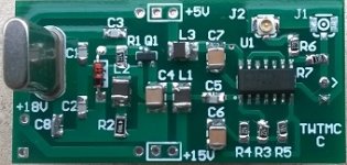
my clock board is almost ready, so I'll open a thread soon.
If someone will be interested I could supply the PCB and the crystal.
This oscillator works with fundamental mode crystal, so the maximum frequency allowed is 25-30 MHz (it will work from 5 to 25-30 MHz simply replacing a couple of caps).
You can see a preview in the attached images.
About using Ian's FIFO buffer with the 1541A core board (recommended), I try to explain my suggestion:
my idea is to sync the source (Ian's FIFO) with the same MCLK of the DAC, to avoid frequency dividers/multipliers, that add jitter themselves.
Since max clock frequency of TDA1541A is 6.4MHz, the only way is to set the frequency of the MCLK at 5.6448 MHz (or 6.144 MHz in case of 48 kHz sample rate).
Using a MCLK at such frequency, it can be placed directly close to the BCK pins of the DAC. The DAC will work at 176.4 kHz, that is almost the maximum frequency allowed.
In that case the DAC works at 128 fs (44.1 * 128 = 5644.8), and since the WS frequency is 44.1 kHz the source must provide 2 words of 64 bit (2 * 64 = 128 fs).
The same MCLK of the DAC will become the MCLK of the source, so Ian's FIFO buffer (the source) should be set to work with that frequency (setting some jumper to 128 fs).
At 128 fs the FIFO, as far as I understand from Ian, will provide 2 words of 64 bit, filling each word with 48 trailing zeros.
The TDA will discard the exceeding bits.
Finally WS and DATA come from FIFO board and BCK from the MCLK. The reclocker board of Ian'S FIFO is not useful in this case, since there is nothing to sync with BCK, since BCK comes directly from the MCLK.
The FIFO buffer acts as an ASRC isolating the real source, so you can use any source (SD card reader, CD tranport, USB to I2S, and so on), without caring about it.
Attachments
About using Ian's FIFO buffer with the 1541A core board (recommended), I try to explain my suggestion:
my idea is to sync the source (Ian's FIFO) with the same MCLK of the DAC, to avoid frequency dividers/multipliers, that add jitter themselves.
Since max clock frequency of TDA1541A is 6.4MHz, the only way is to set the frequency of the MCLK at 5.6448 MHz (or 6.144 MHz in case of 48 kHz sample rate).
.
") Awsome ! Thank you Andrea.
Awsome ! Thank you Andrea.Great, in my case it will be just the I2S to PCM board with no FIFO as it exists some USB to I2S devices with isolator chip and isolated layout...
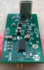
But does the WS and Blck with the I2S to PCM but without FIFO are reclocked as its MCLK is slaved ? That point is not clear for me. My understanding : it is not without the FIFO and if you use a third party USB to I2S : the fs should stay 32 or 64 fs (manual of I2S to PCM) and the result would be great only if this first board of the chain is also slaved by your MCLK ? Right ? Because ifnthere is a drift of the WS and Data in relation to the MCLK which is stable : we have always a jitter problem (ws & data timing given by the source board !)
Does your board allow to slave 3 devices : dac chip + USB to PCM + I2S to PCM with 3 uf.l connectors ? dac chip is slaved with the two pins (stacking), I see one uf.l, but is it possible to add one just near the first (no drift with such conf : more thanvone uf.l ?). On J1 : I can't understand if the empty uf.l trace give the same frequency than the populated uf.l on your photograph ?
Well if the xo is 6.4 max, the max sampling allowed by the I2S to PCM would be 48 hz ! (128 fs minimum for this device)
Good news given by Ben Mah
: uf.l are present for the input on the I2S to PCM board also.
Last edited:
- Status
- This old topic is closed. If you want to reopen this topic, contact a moderator using the "Report Post" button.
- Home
- Source & Line
- Digital Line Level
- Any good TDA1541A DAC kit?