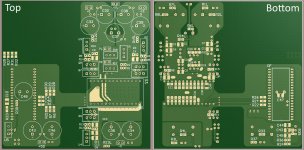
My take on the 1541, work in progress. At least the layout is mine ")
No SPDIF input stage is implemented yet, as i'll try to make it with back-sync to the PC - 2 SPDIF connectors, IN and OUT. With local 384Fs clock source near the DAC.
I haven't connected the DGND, AGND and AGND2 for a reason - they all should be connected together, but i have to try various ground connection schemes first.
As whether i should connect the output ground near the +5V, -15V, or between DEM - or connect the AGND and DGND together near the -5V, or near the AGND pin.
The I2S attenuator/slew limiter will be fine-tuned in place.
No DEM reclocking, as i feel these largish DEM filter caps will clean-up the current much better than the current averaging network made by DEM current source switching. The DEM switching should switch, no matter an what frequency - the "T" of filtering caps in much greater than "T" of the DEM switches.
CXD1244 DF here, as the only one suitable for 1541.
There will be reclock from MCLK (XTAL@384Fs or recovered from SPDIF, user selectable) prior to passing the I2S to the attenuator.
Attachments
Hi,
Digital Filter Chips are jitter central. Abandon all hope on good performance, lest you re-clock the output of the digital filter. Sound quality even after that will be ordinary.
If you must oversample, do it in the PC and use a better quality algorithms than what you find in decade old digital filters.
I think you are seriously mistaking how things work.
DEM reclocking makes sure of two things:
1) Avoid beat tones from interactions between the DEM clock and sample rate, if they are not synchronised
2) Make sure all DEM elements are used for each sample, this means absolute errors may be larger and are not randomised, but relative errors now n \o longer have a random extra error added.
DEM Filter Capacitors filter the switching glitches, which will be at several 100KHz, so we want low ESR and low ESL at those frequencies. Current amounts also vary between the MSB decoupling one sand the lower bits.
Ciao T
The I2S attenuator/slew limiter will be fine-tuned in place.
....
CXD1244 DF here, as the only one suitable for 1541.
Digital Filter Chips are jitter central. Abandon all hope on good performance, lest you re-clock the output of the digital filter. Sound quality even after that will be ordinary.
If you must oversample, do it in the PC and use a better quality algorithms than what you find in decade old digital filters.
No DEM reclocking, as i feel these largish DEM filter caps will clean-up the current much better than the current averaging network made by DEM current source switching.
I think you are seriously mistaking how things work.
DEM reclocking makes sure of two things:
1) Avoid beat tones from interactions between the DEM clock and sample rate, if they are not synchronised
2) Make sure all DEM elements are used for each sample, this means absolute errors may be larger and are not randomised, but relative errors now n \o longer have a random extra error added.
DEM Filter Capacitors filter the switching glitches, which will be at several 100KHz, so we want low ESR and low ESL at those frequencies. Current amounts also vary between the MSB decoupling one sand the lower bits.
Ciao T
DF ain't good nor bad on the jitter front, as long as they are reclocked afterwards. They don't relate to any timings beside data integrity, and as long as no errors are introduced to data, the calculations will be precise on the math frontend. Then i'll shape their math output to external Xtal, and get both precise digital filtering and timing with no loss of bits (as much as possible, given the DF FIR filtering algorithms).Digital Filter Chips are jitter central. Abandon all hope on good performance, lest you re-clock the output of the digital filter. Sound quality even after that will be ordinary.
The PC will be synced with Xtal, therefore everything will be synchronous - no async reclocking with missing bits.
It's a good thing for PC DAC, but everything goes wee when we introduce 176kHz SPDIF. It is quite high sample rate for SPDIF, and really dependant on the SPDIF I/O capabilities on both sides.If you must oversample, do it in the PC and use a better quality algorithms than what you find in decade old digital filters.
Eventually, the 1541 will die with it's 5.6MHz DEM clocking rate, if DEM will be clocked from BCLK.
1.4MHz doesn't seems right for the NOS too. Clock dividers should be used...
I think you are seriously mistaking how things work.
DEM reclocking makes sure of two things:
1) Avoid beat tones from interactions between the DEM clock and sample rate, if they are not synchronised
2) Make sure all DEM elements are used for each sample, this means absolute errors may be larger and are not randomised, but relative errors now n \o longer have a random extra error added.
I think we should split the cases of OS and NOS.
First of all, how many elements we have which are being switched, and how long is their sequential pattern? I guess they aren't random switching, therefore they should form a kind of repeatable pattern, which will affect DAC output - we will see the pattern on the DAC output if we use FFFFFF on I2S, and cycle the DEM with LR clock. To make the DEM switch thru all of the states per single LR clock (given we have DEM sequence length of N), we need Fcosc=N*Fs. Not more not less than multiples of N*Fs.
If we get the clocking wrong, we will get repeatable pattern on DAC output, which will repeat itself, and show-up on THD plot as stick(s).
If we do so, we get N glitches of DEM per sample.
Then let's check the DEM clocking from the aspect of NOS/OS.
NOS has Fs of 44100Hz. The datasheet-recomended frequency for Cosc is around 400kHz, which overclocked, but marginally covered by BCLK/2=700kHz (or BCLK/4=350kHz) given the BCLK=32Fs.
For BCLK/2 we get 16 iterations of DEM, and for BCLK/4 = 8 itertations.
Looks marginally fine, as long as we have 4, 8 or 16 combinations of elements.
For the OS, our Fs goes to 174kHz, and we can't use it's BCLK/2, BCLK/4 for DEM clocking.
Moreover, if we try to stick to Cosc BW limits of no-more-than 700kHz, we are maxed-out by 4*Fs which is still fine for DEM pattern length of 4. But if we have more than 4 combinations of elements, we don't benefit from per-sample averaging of elements. Say we have 8-cycle combination of elements and 4*Fs clock. Then 1st sample on DAC output will use average from first 4 combinations, and 2nd sample will use 4 other combinations. We get a square wave of Fs/2 on DAC output, which is bad.
On the other hand, if we go with free-running DEM clk, we get some randomness of switching per every sample. It's noise distributes over the spectrum, and we may even benefit from it as from "dithering".
To clearly see the DEM pattern, i think we should remove the DEM filtering caps.
4.7uF X7R 1206 is ok in ESR/ESL domain? Their leakage current should be concerned too...DEM Filter Capacitors filter the switching glitches, which will be at several 100KHz, so we want low ESR and low ESL at those frequencies. Current amounts also vary between the MSB decoupling one sand the lower bits.
Here is an article about DEM, dated 1976
http://overture.org.ua/wp-content/uploads/2011/09/00046328.pdf
I need to read it prior to arguing
http://overture.org.ua/wp-content/uploads/2011/09/00046328.pdf
I need to read it prior to arguing
Hi,
Agreed, yet I seem to have missed the re-clocker in your schematic and on your PCB...
Quad speed SPDIF that locks reliably is now very common. There are chip's from almost any maker. And why not use Quad Speed I2S vias USB?
If you read my earlier notes, I agree on using a Dividier for DEM reclocking.
Why? How does the DAC distinuish between being fed 44.1KHz upsampled to 176.4KHz and being feed a non-oversampled 176.4KHz signal?
It's in the TDA1541 extended info datasheets...
Correct.
Maybe. From experience ceramic should not be used here. Use SMD stacked Film, many options now.
Ciao T
DF ain't good nor bad on the jitter front, as long as they are reclocked afterwards.
Agreed, yet I seem to have missed the re-clocker in your schematic and on your PCB...
It's a good thing for PC DAC, but everything goes wee when we introduce 176kHz SPDIF.
Quad speed SPDIF that locks reliably is now very common. There are chip's from almost any maker. And why not use Quad Speed I2S vias USB?
Eventually, the 1541 will die with it's 5.6MHz DEM clocking rate, if DEM will be clocked from BCLK. 1.4MHz doesn't seems right for the NOS too. Clock dividers should be used...
If you read my earlier notes, I agree on using a Dividier for DEM reclocking.
I think we should split the cases of OS and NOS.
Why? How does the DAC distinuish between being fed 44.1KHz upsampled to 176.4KHz and being feed a non-oversampled 176.4KHz signal?
First of all, how many elements we have which are being switched, and how long is their sequential pattern?
It's in the TDA1541 extended info datasheets...
I guess they aren't random switching, therefore they should form a kind of repeatable pattern, which will affect DAC output - we will see the pattern on the DAC output if we use FFFFFF on I2S, and cycle the DEM with LR clock. To make the DEM switch thru all of the states per single LR clock (given we have DEM sequence length of N), we need Fcosc=N*Fs. Not more not less than multiples of N*Fs.
Correct.
4.7uF X7R 1206 is ok in ESR/ESL domain? Their leakage current should be concerned too...
Maybe. From experience ceramic should not be used here. Use SMD stacked Film, many options now.
Ciao T
Probably you have missed the:Agreed, yet I seem to have missed the re-clocker in your schematic and on your PCB...
There will be reclock from MCLK (XTAL@384Fs or recovered from SPDIF, user selectable) prior to passing the I2S to the attenuator.
The reclocker was missing because i haven't yet decided which IC to use, and which casing. DIP will look on par with DF and DAC, but a bit clunky.
SOICs are techie, but prevent a nice bypassing under the IC due to VIAs.
I like the way pins are arranged in 574 IC of 74 family. It's quad DFF with positive outputs only, and it has inputs and outputs on opposite edges.
ABT/BCT? BiCMOS looks attractive from propagation delay and power usage points of view...
USB-slave is really nice option, but it is USB, and i'm not aware of publically available, cost effective AND easily implementable ICs, which doesn't require FPGAs, MCUs and preflashing.Quad speed SPDIF that locks reliably is now very common. There are chip's from almost any maker. And why not use Quad Speed I2S vias USB?
SPDIF@174kHz? The issus with SPDIF "as-is" is unresolvable thus requiring us to use reclocking + back-syncing.
I'll try to run my project with oversampling @PC + DF bypass, but i'm uncertain whether i'll be able to make the back-sync thing work at 174kHz.
Without back-syncing it gets even worse as the sampling frequency rises...
It won't distinguish as long as Fs=176.4KHz is on 1541's inputs.Why? How does the DAC distinuish between being fed 44.1KHz upsampled to 176.4KHz and being feed a non-oversampled 176.4KHz signal?
Yet, the BCLK divider for DEM clocking at Fs=44.1k and Fs=176.4k should be different, otherwise DAC will distinguish the change in a bad manner
Every time i hear "NOS" i think of DAC running at Fs=44100Hz.
As long as we upsample the signal at some point of digital chain, the whole system shouldn't be called "NOS".
I'll take closer look at these sheets. (Are they from IEEE?)It's in the TDA1541 extended info datasheets...
SMT PPS die when you touch them with soldering ironMaybe. From experience ceramic should not be used here. Use SMD stacked Film, many options now.
Lots of care should be taken at soldering time, otherwise we'll hear clicking noises on DAC output when the music hits missing bits.What about my grounds layout?
I didn't liked the capacitive/inductive coupling of DGND and AGND when they are on top of each other (2-layers), so i decided to move the DGND aside.
By doing this i halved the AGND impedance, got solid AGND layer
But i've got a half-circle loop between -5V and DGND pins with -5V PSU in between. The DAC chip is in center of EMI field produced by currents flowing from -5 to DGND and back given the "right hand rule" is true
.Hi,
I looked at the schematic and PCB, sorry.
Personally I don't even bother starting on the PCB until I have the basics sorted and maybe breadboarded any stuff I'm not sure will work.
You could buy something off the shelf (M2-Tech thingey?) and mod it. Not that hard.
But you said you would do that, so where is the problem?
Use Asynchronous USB.
Why. As long as the minimum of full cycles happen at 176.4KHz it will be fine. At 176.4KHz and at 44.1KHz (Non-OS).
I don't. I think of a DAC running at 1Fs, with FS being anything the DAC can handle (for TDA1541 that would be 384KHz in duplex mode).
As the late Steve Jobs so famously said to 21 Million iPhone 4 users that complained calls dropped if they held their phone in a certain way: "Then just don't do that!".
Your call, we all have our preferences.
Ciao T
Probably you have missed the:
I looked at the schematic and PCB, sorry.
Personally I don't even bother starting on the PCB until I have the basics sorted and maybe breadboarded any stuff I'm not sure will work.
USB-slave is really nice option, but it is USB, and i'm not aware of publically available, cost effective AND easily implementable ICs, which doesn't require FPGAs, MCUs and preflashing.
You could buy something off the shelf (M2-Tech thingey?) and mod it. Not that hard.
SPDIF@174kHz? The issus with SPDIF "as-is" is unresolvable thus requiring us to use reclocking + back-syncing.
But you said you would do that, so where is the problem?
I'll try to run my project with oversampling @PC + DF bypass, but i'm uncertain whether i'll be able to make the back-sync thing work at 174kHz. Without back-syncing it gets even worse as the sampling frequency rises...
Use Asynchronous USB.
Yet, the BCLK divider for DEM clocking at Fs=44.1k and Fs=176.4k should be different,
Why. As long as the minimum of full cycles happen at 176.4KHz it will be fine. At 176.4KHz and at 44.1KHz (Non-OS).
Every time i hear "NOS" i think of DAC running at Fs=44100Hz.
I don't. I think of a DAC running at 1Fs, with FS being anything the DAC can handle (for TDA1541 that would be 384KHz in duplex mode).
SMT PPS die when you touch them with soldering iron
As the late Steve Jobs so famously said to 21 Million iPhone 4 users that complained calls dropped if they held their phone in a certain way: "Then just don't do that!".
What about my grounds layout?
Your call, we all have our preferences.
Ciao T
Thorsten,
I want to use some SPDIF-like transformer to isolate the Cosc pins from reclocking circuit.
Should i still tie the Cosc pins to -15v with 2k2 resistors? I don't like the idea of polluting the -15v line with digitallish signal, even thru relatively high resistors. I guess i'll need to split the -15v line to two -15 sources, unless there is alternative solution for DEM clocking signal feed.
Also i find it crude to pull Cosc pins to -15v
And i guess pulling the isolated trafo windings to -15v won't work, probably i need to tie the cosc pins between -15v and somewhere at +/-5v.
By the way, if we get constant averaging of current source variations with DEM clocking, then we will get constant sample-to-sample DEM averaged current delivered to each bit.
Then we could introduce leakage current to each bit by tying the DEM filtering caps somewhere, say GND with trimmer resistors.
Then we could be able to fine-tune the current for each available bit.
Yay? Access to bit tuning of bits...
Hi,
Frequency may be too low and impedance too high to use SPDIF Transformers.
The DEM reclocking by ecdesigns that I recommend is balanced, so not much net current, if you want to loose sleep over it add a choke and local decoupling, though given the actual internal TDA1541 schematic I think this could be counter-productive.
Tell that to Rudy Van Plasche. He designed the TDA1540 and TDA1541 that way.
Yes, I think you could monkey with that, but I doubt there is much to be gained that way.
Ciao T
I want to use some SPDIF-like transformer to isolate the Cosc pins from reclocking circuit.
Frequency may be too low and impedance too high to use SPDIF Transformers.
The DEM reclocking by ecdesigns that I recommend is balanced, so not much net current, if you want to loose sleep over it add a choke and local decoupling, though given the actual internal TDA1541 schematic I think this could be counter-productive.
Also i find it crude to pull Cosc pins to -15v
Tell that to Rudy Van Plasche. He designed the TDA1540 and TDA1541 that way.
By the way, if we get constant averaging of current source variations with DEM clocking, then we will get constant sample-to-sample DEM averaged current delivered to each bit.
Then we could introduce leakage current to each bit by tying the DEM filtering caps somewhere, say GND with trimmer resistors.
Then we could be able to fine-tune the current for each available bit.
Yay? Access to bit tuning of bits...
Yes, I think you could monkey with that, but I doubt there is much to be gained that way.
Ciao T
Ok, i've got proof-of-concept circuit working, for back-syncing with single WM8804 in simultaneous transmit/receive mode, HW configged.
SPDIF Back Sync
It will work the moment i'll add XTAL with MCLK divider to get BCLK/LRCLK clocks, and feed them to both DF (TDA for NOS) and WM8804.
I'll check the solution for 96kHz this evening (max speed of DIR9001 i use for generating clocks which i feed to the WM).
44.1/48 works flawlessly.
SPDIF Back Sync
It will work the moment i'll add XTAL with MCLK divider to get BCLK/LRCLK clocks, and feed them to both DF (TDA for NOS) and WM8804.
I'll check the solution for 96kHz this evening (max speed of DIR9001 i use for generating clocks which i feed to the WM).
44.1/48 works flawlessly.
Hi,
Can you provide proof of this? Well, proof of the contrary is in March 2012 Stereophile.
A DAC I designed with passive I/V and Tube gain stages is tested by JA in Stereophile March 2012 and shows appx. -135dB FFT Noisefloor with 24-Bit Signals (I am sure you can work backwards to the ENOB from this easily).
So tubes DO deliver 16 Bit resolution just fine (and yet another of your claims has been illustrated to be incorrect).
Ciao T
Hello Thorsten
I've take a look today at the Stereophile web site and I can't find those tests.
Can you tell me, please, where they are in the Stereophile web site ?
Thank you
Bye
Gaetan
Last edited:
Hi,
They are in the March issue (print).
Ciao T
I've take a look today at the Stereophile web site and I can't find those tests.
Can you tell me, please, where they are in the Stereophile web site ?
They are in the March issue (print).
Ciao T
Hi,
I wrote -135dB FFT Noise Floor. So what you write is Bull...
If you paid attention in the relevant classes you know how these measurements work and you can work backwards from this to ENOB.
THD itself is meaningless, Noise is derivative of the above. So more bull.
Ciao T
-135dB noise floor is bull. It's because shorted outputs probably and that is just the ADC noise. Anyway, irrelevant.
I wrote -135dB FFT Noise Floor. So what you write is Bull...
If you paid attention in the relevant classes you know how these measurements work and you can work backwards from this to ENOB.
One of the relevant/important measurements is THD+N at 0dB and -60dB. That shows the actual audio resolution of a certain device.
THD itself is meaningless, Noise is derivative of the above. So more bull.
Ciao T
Thorsten, have you tried different passive filtering options prior to I/V convertion?
The issue with most I/V stages with feedback (and others too) is that their input impedance rises with a frequency, failing at voltage compliance and other troubles for HF noise. Moreover, HF noise ain't good for anything.
How about inductor to I/V with matching cap to GND (or thru matching resistor, to match input impedance of I/V, to GND)? Kinda speaker's crossover with flat impedance for DAC, and frequency splitting to GND and I/V?
By the way, my back-sync works with 96kHz too. I don't have 192kHz source to test it, and there is almost no soundcards with 192kHz input.
Last edited:
I wrote -135dB FFT Noise Floor.
Yeah but unless SoNic is clairvoyant, he's not going to be able to work out the 22kHz bandwidth noise unless you tell us the effective bin bandwidth. Does the original article divulge this important snippet?
Number of bins, no. of averages, sample rate and the ****-factor arising from the windowing function pretty please?
Hi,
I normally incorporate passive filtering (1st Order) with the passive I/V, similar to the capacitor in parallel with the I/V resistor in Op-Amp I/V.
For Op-Amp I/V I usually use CFB Op-Amp's, or if not I use VFB Op-Amp's I use the Wurcer Trick (cap from -in to ground) and Op-Amp's that are not unity gain stable. You might call that "pre-filtering", though it actually works differently.
Ciao T
Thorsten, have you tried different passive filtering options prior to I/V convertion?
I normally incorporate passive filtering (1st Order) with the passive I/V, similar to the capacitor in parallel with the I/V resistor in Op-Amp I/V.
For Op-Amp I/V I usually use CFB Op-Amp's, or if not I use VFB Op-Amp's I use the Wurcer Trick (cap from -in to ground) and Op-Amp's that are not unity gain stable. You might call that "pre-filtering", though it actually works differently.
Ciao T
Hi,
Indirectly.
Stereophile always measures the same way over decades now and you can use this data for comparison and work out the correction factors.
In fact, our friend SoNic illustrated not only that he does not understand the difference between noisefloor and FFT noisefloor.
He also illustrated that he never looked at the article referenced and simply declared something to be bull-.... based on his lack of understanding basic electronics and his prejudices against tubes, instead of making an intelligent contribution to the thread or instead of providing proof that my assertions where wrong.
Ciao T
Yeah but unless SoNic is clairvoyant, he's not going to be able to work out the 22kHz bandwidth noise unless you tell us the effective bin bandwidth. Does the original article divulge this important snippet?
Indirectly.
Stereophile always measures the same way over decades now and you can use this data for comparison and work out the correction factors.
In fact, our friend SoNic illustrated not only that he does not understand the difference between noisefloor and FFT noisefloor.
He also illustrated that he never looked at the article referenced and simply declared something to be bull-.... based on his lack of understanding basic electronics and his prejudices against tubes, instead of making an intelligent contribution to the thread or instead of providing proof that my assertions where wrong.
Ciao T
Thorsten, have you tried different passive filtering options prior to I/V convertion?
As a relative noob to the I/V malarky, I'll just mention what I'm playing with at the moment as a kind of counterbalance to Thorsten.
I flirted with cap to ground but didn't much like the sound on TDA1543 or TDA1545. I'm not really sure why this would tend to flatten the sound stage, but that was the effect. On TDA1543 the effect was mitigated by using an external current source (set the internal bias to zero). I decided to take the dual, which is a series inductor (after the I/V resistor) and that's been giving me more listening pleasure of late. But I'm doing this in differential mode, with digital inversion and more than one DAC chip.
The series inductor I chose was one with a high SRF (above 200MHz) intended for use as a CM choke. I agree that HF noise is the big bug-bear and DACs create a lot - especially CMOS DACs like the TDA1545.
- Status
- This old topic is closed. If you want to reopen this topic, contact a moderator using the "Report Post" button.
- Home
- Source & Line
- Digital Line Level
- Any good TDA1541A DAC kit?