I've spent another minute thinking about it.
You probably want such a starting point for your special details like exact capacitor size, exact resistor and connector placement, etc.
The board is single sided, 1" wide by 1.65" long and could still be shrinked, if neccessary (not recommended). I'd suggest you implement some mounting holes, as the board should never hang off the IC pins! I'll leave it for you to find matching holes in the library 'holes' and place them on the board...")
You probably want such a starting point for your special details like exact capacitor size, exact resistor and connector placement, etc.
The board is single sided, 1" wide by 1.65" long and could still be shrinked, if neccessary (not recommended). I'd suggest you implement some mounting holes, as the board should never hang off the IC pins! I'll leave it for you to find matching holes in the library 'holes' and place them on the board...
Attachments
PS: Now it's time for everybody to jump in and improve the actual circuit before the board can get 'finished'.
Yes, for example the signal ground input should go to circuit ground, not the non-inverting input!
Hi sek-
Thanks for the redirection to yarg. I started reading the thread but have a little left to go. Looks intresting but my project requires multiples of the LM3886 chips. You care to redraw your board with a slim-line profile, 2 LM3886's and the regulator?
Also you mention...
"Well, I've thougt about it for a minute."
"I've spent another minute thinking about it."
Smart A$$. I've been thinking about how to draw that in Eagle for over a week...
I will REQUEST a few modifications in the morning but the wife says it is time to tuck the kids in.
I really appreciate what you've done. I had that in my head for a month now but couldn't put it on Eagle. I can draw it in Visio, and ExpressPCB, but I'm too new to Eagle.
What I am attempting is "slime-line" PCB's so you can place multiples side-by-side and parallel or bridge them as needed.
The next revision will have two of the LM3886 "boards with a reg and be the width of slightly wider than all three chips together.
Thanks for the redirection to yarg. I started reading the thread but have a little left to go. Looks intresting but my project requires multiples of the LM3886 chips. You care to redraw your board with a slim-line profile, 2 LM3886's and the regulator?
Also you mention...
"Well, I've thougt about it for a minute."
"I've spent another minute thinking about it."
Smart A$$.
I've been thinking about how to draw that in Eagle for over a week...I will REQUEST a few modifications in the morning but the wife says it is time to tuck the kids in.
I really appreciate what you've done. I had that in my head for a month now but couldn't put it on Eagle. I can draw it in Visio, and ExpressPCB, but I'm too new to Eagle.
What I am attempting is "slime-line" PCB's so you can place multiples side-by-side and parallel or bridge them as needed.
The next revision will have two of the LM3886 "boards with a reg and be the width of slightly wider than all three chips together.
Now I see why you sent me a note.
What are your enclosure requirements?
The amp boards I have are 1"x1.5" roughly (no regs) or 1"x3" with regs on-board. And I think putting the regs at the chip is the way to go in this case because you shouldn't put more than 2 chips on a pair of LM338 regs. Doing this means you can run a whole mess off a properly sized transformer/rectifier/cap setup.
This can still fit in a 2" tall case with the right heat-sink.
The electronics don't care how they're oriented. The heat sink does. Even though I have a 3" wide design, it'll fit in a 2" tall case. And you could wire up a whole pile fairly simply to make a parallel amp, bridge amp, etc. I don't have bridging circuits yet.
Stop being constrained by tradition.
C
Hi,
The more interesting part is in the last couple of posts. But reading the whole thread helps to understand my reasoning, the most important being: size constraints (mostly depht, not width).
That tells me you haven't read it through, yes
The project was actually born because I needed an option to combine multiple units in a single enclosure of very constrained size. That's why it is small, slim and stackable
That's like starting a new project, really...
I think you're better off learning to get comfortable with eagle, it's rather easy once you get used to the fact that it's a unix program without wind*ws-conformity...
Great I could help.
Why do you switch to Eagle anyway?
Would probably be the easiest to have two types of modules then, (1) power supply with rectifier, filter and regulators and (2) single channel LM3886 board, both with the same form factor. You could then combine them the way you like... Just a thought.
A symmetrical supply needs two regulators, that's four ICs per two-channel unit.
1.2" x 3" is about the size of the mentioned yarg project boards, stackable (have you two considered the 3rd dimension yet?). You could reduce the schematic by everything that's unneccessary for you (e.g. the input filter, output filter, regulator protection and some more optional components; but I don't recommend that!) and then rearrange the components to your needs. Less work than starting it all from scratch... Just another thought
The LM338 is a good, old, inexpensive way to go. However, I always like to recommend the LT108x series (linear.com). The LT1083 is capable of supplying twice the power of the LM338 while regulating better, dissipating less quiescent power (quasi-LDO) and staying cooler (in it's TO274 case). That means twice the number of channels per regulator. The cost for the LT1083 is higher than that for the LM338, but saving a whole extra regulator board per LM338 reduced pays off at more than one.
Think about it, you probably don't need as many regulators as you think.
Is 2" your size constraint? I wonder what heat sink can sink (short term, thick base plate) and dissipate (long term, large fin surface) the power of more than a couple of LM3886 channels (>60W each!). If the mentioned 3" are available, the stackable boards (between 1" and 2" height per unit) could be oriented vertically and then mounted horizontally. That makes for between 20 and 40 channels (depending on the number of amps per regulator) per 19" form factor enclosure for the dual-channel board version, for example.
If you use active cooling, of course!
I wouldn't recommend packing the LM3886 too tight into a small enclosure and especially onto a small (passive) heatsink. I have calculated this through in another thread (my contribution to the topic starts from posting #22).
It's actually interesting what safe operating area power dissipation one has to consider. It was ca. 140W for two channels, including two regulators per amplifier channel!
Not to be overlooked when driving low impedances and/or high powers out of a bridged/parallel gainclone! Especially with kids around the unit...
But I'll stop at this point, everybody has to decide such things individually. Just one thing: Please make shure you've read and understood e.g. the Gainclone safety thread or something alike. It's not sensible to make power circuits as small as physically possible. With a 2" tall enclosure, as tight around the circuitry as possible (and with an adventurous heatsink) would have to be equipped with fans so big (and/or loud) that the whole miniaturization is seriously questioned.
Sebastian.
rabstg said:Thanks for the redirection to yarg. I started reading the thread but have a little left to go.
The more interesting part is in the last couple of posts. But reading the whole thread helps to understand my reasoning, the most important being: size constraints (mostly depht, not width).
Looks intresting but my project requires multiples of the LM3886 chips.
That tells me you haven't read it through, yes
The project was actually born because I needed an option to combine multiple units in a single enclosure of very constrained size. That's why it is small, slim and stackable
You care to redraw your board with a slim-line profile, 2 LM3886's and the regulator?
That's like starting a new project, really...
I think you're better off learning to get comfortable with eagle, it's rather easy once you get used to the fact that it's a unix program without wind*ws-conformity...
Smart A$$.
I really appreciate what you've done. I had that in my head for a month now but couldn't put it on Eagle. I can draw it in Visio, and ExpressPCB, but I'm too new to Eagle.
Great I could help.
Why do you switch to Eagle anyway?
What I am attempting is "slime-line" PCB's so you can place multiples side-by-side and parallel or bridge them as needed.
Would probably be the easiest to have two types of modules then, (1) power supply with rectifier, filter and regulators and (2) single channel LM3886 board, both with the same form factor. You could then combine them the way you like... Just a thought.
The next revision will have two of the LM3886 "boards with a reg and be the width of slightly wider than all three chips together.
A symmetrical supply needs two regulators, that's four ICs per two-channel unit.
cjd said:The amp boards I have are 1"x1.5" roughly (no regs) or 1"x3" with regs on-board.
1.2" x 3" is about the size of the mentioned yarg project boards, stackable (have you two considered the 3rd dimension yet?). You could reduce the schematic by everything that's unneccessary for you (e.g. the input filter, output filter, regulator protection and some more optional components; but I don't recommend that!) and then rearrange the components to your needs. Less work than starting it all from scratch... Just another thought
And I think putting the regs at the chip is the way to go in this case because you shouldn't put more than 2 chips on a pair of LM338 regs. Doing this means you can run a whole mess off a properly sized transformer/rectifier/cap setup.
The LM338 is a good, old, inexpensive way to go. However, I always like to recommend the LT108x series (linear.com). The LT1083 is capable of supplying twice the power of the LM338 while regulating better, dissipating less quiescent power (quasi-LDO) and staying cooler (in it's TO274 case). That means twice the number of channels per regulator. The cost for the LT1083 is higher than that for the LM338, but saving a whole extra regulator board per LM338 reduced pays off at more than one.
Think about it, you probably don't need as many regulators as you think.
This can still fit in a 2" tall case with the right heat-sink.
Is 2" your size constraint? I wonder what heat sink can sink (short term, thick base plate) and dissipate (long term, large fin surface) the power of more than a couple of LM3886 channels (>60W each!). If the mentioned 3" are available, the stackable boards (between 1" and 2" height per unit) could be oriented vertically and then mounted horizontally. That makes for between 20 and 40 channels (depending on the number of amps per regulator) per 19" form factor enclosure for the dual-channel board version, for example.
If you use active cooling, of course!
I wouldn't recommend packing the LM3886 too tight into a small enclosure and especially onto a small (passive) heatsink. I have calculated this through in another thread (my contribution to the topic starts from posting #22).
It's actually interesting what safe operating area power dissipation one has to consider. It was ca. 140W for two channels, including two regulators per amplifier channel!
Not to be overlooked when driving low impedances and/or high powers out of a bridged/parallel gainclone!
Especially with kids around the unit... But I'll stop at this point, everybody has to decide such things individually. Just one thing: Please make shure you've read and understood e.g. the Gainclone safety thread or something alike. It's not sensible to make power circuits as small as physically possible. With a 2" tall enclosure, as tight around the circuitry as possible (and with an adventurous heatsink) would have to be equipped with fans so big (and/or loud) that the whole miniaturization is seriously questioned.
Sebastian.
sek:
Your project is very similar, but also different, to what I have come up with so far. I found routing the power in on one side to allow more flexibility for me, but that put the regs on one end of the board (one on each side). Interesting to see all the different solutions to the same basic problem though.
3rd dimension? Yes. Long ago. Well, if four months ago counts as "long ago". Relative to my time with this aspect of the hobby, that's a good while.
2" includes a 1" heatsink. Put it on top, and convection will draw the heat. But, that's just a rough figure, and probably not realistic.
And, I'm looking at two applications: 7 channels bridge-parallel, and tri-amped speakers. The former is, I believe, 42 chips. The latter, I'm not sure. If I ever get around to it. Looking at all the various ways to get entirely too confused in assembling is what finally suggested to me that putting regs at each chip was the way to go. That also keeps connections short, which is also a benefit I believe.
It is entirely probable that I am missing something.
C
Your project is very similar, but also different, to what I have come up with so far.
I found routing the power in on one side to allow more flexibility for me, but that put the regs on one end of the board (one on each side). Interesting to see all the different solutions to the same basic problem though.3rd dimension? Yes. Long ago. Well, if four months ago counts as "long ago".
Relative to my time with this aspect of the hobby, that's a good while.2" includes a 1" heatsink. Put it on top, and convection will draw the heat. But, that's just a rough figure, and probably not realistic.
And, I'm looking at two applications: 7 channels bridge-parallel, and tri-amped speakers. The former is, I believe, 42 chips. The latter, I'm not sure. If I ever get around to it.
Looking at all the various ways to get entirely too confused in assembling is what finally suggested to me that putting regs at each chip was the way to go. That also keeps connections short, which is also a benefit I believe.It is entirely probable that I am missing something.
C
cjd said:Your project is very similar, but also different, to what I have come up with so far.
Yeah, that's true. I don't particularly 'love' my design, it just seems to be the most practical for the purpose.
2" includes a 1" heatsink. Put it on top, and convection will draw the heat.
Now that's small
That subtracts to 1" for the whole amplifier unit, did I get that right? So, no large capacitors near the chipamp? Yes, should work well with a regulated supply. Does it work stable with multiple units connected to a single regulator (pair) via long wires?
But, that's just a rough figure, and probably not realistic.
Probably not, because the amount of heat a 1" aluminium spreader can dissipate only depends on the fin surface. Without a fan, it would have to be a surreal extrusion profile. I guess you're describing multiple amp modules sharing a common heatsink (having 1" depth)? Even that is not enough, at least if the sink is well 'populated'.
And, I'm looking at two applications: 7 channels bridge-parallel, and tri-amped speakers. The former is, I believe, 42 chips. The latter, I'm not sure. If I ever get around to it.
Now that's a number. 42 chips (I assume 6 chips BPA per channel), all installed in a safe manner, would dissipate about 2.5kW, not accounting for losses and the regulators. The PSU probably won't supply that over a long term, so it is the limiting factor. You'd have to install heat sinks suitable to dissipate all the power your PSU can supply...
Looking at all the various ways to get entirely too confused in assembling is what finally suggested to me that putting regs at each chip was the way to go. That also keeps connections short, which is also a benefit I believe.
Well let's say you go for a certain average power level. You could dissipate a reasonable power over a 1" sink area per chipamp, but it won't be too high. So why BPA with 6 chips per channel. Once they have to supply current, they heat up. Even so the regulators, and you would need many of them (2 * 42 = 84 pieces at about 5$ each!). It seems there's a reason why most manufacturers use discrete circuits in AV amps, it's just not the right application for chipamps. Consider the sound, not only how much peak power you can draw out of a channel (the average power, drawn out of all channels at once, would then overload the PSU and/or the heat sink).
OTOH, don't let yourself get fooled out of your ideas by a stranger
Just make sure to keep it safe. And keeping good sound quality (while preventing failure due to overload) seems to be your biggest concern...
Cheers,
Sebastian.
Mostly just having fun dreaming, and trying to learn what's what. It all started as something to keep me occupied and my spirits up while I was unemployed earlier this summer.
With the regs at the chip it would just be requiring a sufficient torroid, rectifier, and capacitor bank. I think. If I'm understand what I'm reading, and it is entirely too possible that I don't understand everything I need to. One of my ideas includes mounting the large PS caps near the chip boards - think a bars for each rail, mount amp boards to one side and caps to the other. Not sure. I suspect putting the large PS caps far away from the regs isn't as good an idea.
As for regs, it would be most efficient for me to get 100 from digikey for $115.60usd to supply 42 chips. And have a few left over for some simpler projects. $151 for chips (less if I buy 100 and sell extras or use them elsewhere), who knows what for torroid(s), caps, and the rest... it'll probably push close to the cost of something like an Outlaw 770 (which, for HT, probably sounds plenty good). But I'll have made it, and it can look however I want it to look. Plus, I'll have made it. And, did I mention the satisfaction of having made it myself?
Heat sinks, I have actually been considering some different strategies. One that seems like it may be odd, but sensible, would be to use some of the better low-cost units intended for computers. Two chip boards could share a HS, or it could be cut to cover two individually.
And, I have no problem with active cooling either. I'm getting pretty good at keeping air moving it a very low noise level in my computers (not good enough yet, but getting better).
After all this, I may never really get around to any of it.
C
With the regs at the chip it would just be requiring a sufficient torroid, rectifier, and capacitor bank. I think. If I'm understand what I'm reading, and it is entirely too possible that I don't understand everything I need to.
One of my ideas includes mounting the large PS caps near the chip boards - think a bars for each rail, mount amp boards to one side and caps to the other. Not sure. I suspect putting the large PS caps far away from the regs isn't as good an idea.As for regs, it would be most efficient for me to get 100 from digikey for $115.60usd to supply 42 chips.
And have a few left over for some simpler projects. $151 for chips (less if I buy 100 and sell extras or use them elsewhere), who knows what for torroid(s), caps, and the rest... it'll probably push close to the cost of something like an Outlaw 770 (which, for HT, probably sounds plenty good). But I'll have made it, and it can look however I want it to look. Plus, I'll have made it. And, did I mention the satisfaction of having made it myself? Heat sinks, I have actually been considering some different strategies. One that seems like it may be odd, but sensible, would be to use some of the better low-cost units intended for computers. Two chip boards could share a HS, or it could be cut to cover two individually.
And, I have no problem with active cooling either. I'm getting pretty good at keeping air moving it a very low noise level in my computers (not good enough yet, but getting better).
After all this, I may never really get around to any of it.
C
Hi sek-
I have a couple of questions on how to modify the slime-line PCB you drew for me.
First off I really want to thank you for your time. The PCB you drew was exactly what I was trying to do.
The PCB can use top and bottom layer since it will be made at a factory. Also the components (except the supply +- V caps) can be placed on top AND bottom.
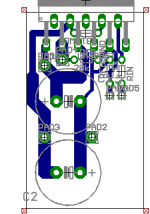
1. How do I move pad 3 to the left a little more to straighten out the trace from C2?
2. How do you move pad 5 (and the one next to it) and Rin to the right? I also will move the trace to the top layer.
3. Can you add 2 output resistors to parallel multiple boards?
4. Separate traces as much as possible but alternating top and bottom layers.
5. Widen traces as much as possible?
6. The board can be lengthened to give you more room in front of the chip.
I have a couple of questions on how to modify the slime-line PCB you drew for me.
First off I really want to thank you for your time. The PCB you drew was exactly what I was trying to do.
The PCB can use top and bottom layer since it will be made at a factory. Also the components (except the supply +- V caps) can be placed on top AND bottom.
1. How do I move pad 3 to the left a little more to straighten out the trace from C2?
2. How do you move pad 5 (and the one next to it) and Rin to the right? I also will move the trace to the top layer.
3. Can you add 2 output resistors to parallel multiple boards?
4. Separate traces as much as possible but alternating top and bottom layers.
5. Widen traces as much as possible?
6. The board can be lengthened to give you more room in front of the chip.
Attachments
For gits and shiggles...
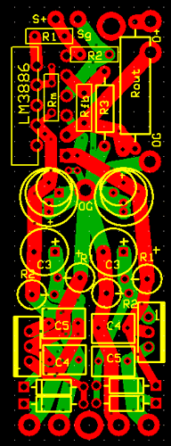
I have an inverted chip-amp layout that'll sit in place of the NI layout with all the inputs/outputs in exactly the same spots.
1 inch wide, 2.9 inches long.
I have not yet verified 100% that this is actually entirely compliant with the schematic, but I'm 99% sure at this point.
C
I have an inverted chip-amp layout that'll sit in place of the NI layout with all the inputs/outputs in exactly the same spots.
1 inch wide, 2.9 inches long.
I have not yet verified 100% that this is actually entirely compliant with the schematic, but I'm 99% sure at this point.
C
Hi,
That sounds good, glad I could really help (and not only try).
I've read in another thread that you're away over the weekend. I guess you're reading this later, so I'll sort out a couple of things first.
No problem, but look how you drive me into doing it for you again (in the step between question 1 and 2):
Funny
I don't state this because I'm lazy or don't care. I just don't know your situation as good as you do. See, sorting everything out, making sure you know every measure, every constraint, every part of the plan, and such; this is all much more work (and fun) than doing a small layout. Thus, while you have the plan, I can only quess what you want exactly. However, I won't let you alone on this!
Every little lack of information on my side could lead to a serious amount of work in order to correct for 'design changes' that have to be done after a correction.
That said, all we have to do is clear all the important issues to get this first sketch into a working building block. Let's see what we (both) know and what we (me in terms of information, you in terms of solution) need:
This is good news, as you (and Steve, for that matter, whoever he is) don't have to fiddle around with processing/etching something from someone else's work (which is always difficult, as every DIYer has own preferences on how to prepare photo films and such).
OTOH, commercial board manufacturers usually specify:
- what data they need (supposedly either gerber files, a foil image or project files),
- what limitations their manufacturing process has (i.e. minimum distances, wire widths, drill sizes, etc.),
- what they recommend in order to help reduce production cost (like wether you're allowed to align multiple boards for later cutting apart; and if so, how...).
It would be great if you found this out first; either look at the web site of the board house or mail them for e.g. a CadSoft Eagle 'design rule' file.
Yes, that would be my next question: How much space is around each board?
You probably have a sketch or a drawing?
As there are only caps, resistors and the chip, it's clear which components can also be placed on the bottom layer: the resistors.
By using the command 'move'? No, kidding. I'll do that once everything else is pointed out.
Such as: which components do you actually intend to use?
This mainly has to do with grid (pin distance), diameter and distance/spacing.
Most important to know are the supply capacitors and the 'power' resistors.
For the capacitors, I assumed the smallest 1000uF/35V type that is available to me, for the resistors I don't know.
But please keep in mind: for bridging/paralleling, you'd need high precision resistors that probably don't come in standard 0207 size.
Same answer as above: once every component is determined, this will be no problem for me. I'm looking at your picture to see the direction you want everything to go.
Now this is really something new: I'm not sure wether I understand your question right, because I have no schematic to start from. I used the one you posted, but it was neither correct, nor complete...
I guess we're talking about BR100, PA100, BPA200 as of National's AN-1192. The thing I clicked together doesn't really match their core building block yet.
Even the simplified circuit as of AN1192's Figure 17 requires the capacitors Ci, I would therefore recommend to reserve space for them.
Also, the recommended supply in Figure 16 doesn't require large supply bypass capacitors for each chip. You already said that you'll have a large capacitor 'block' in the power supply, so we can probably minimize the supply capacitors on the board. The regulated supply you probably want to implement in a later stage won't require significant capacitance near the chip amps at all...
The LM3886's datasheet requires (or highly recommends) a capacitor at the mute pin in order to prevent turn-on pops; have you thought about this yet?
This will become easier now that I have two layers available.
The first attempt had too slim and too narrow traces; after all, it was just a first attempt...
Good. I assume the available length will be shown in your drawing.
What about the regulators? Will they have to be designed, too? (Easy...!?)
In this regard, it would help to know your actual application, e.g. what purpose(s) the finished amp will be used for.
Also, we forgot mounting the board itself so far. It needs holes and the screws through them have to hold somewhere in your enclosure!
Anoter point: think about the positions of every connector, you'll have to be able to reach them on all the boards inside the enclosure, and I guess it will be very tight in there once everything is mounted.
Okay, that's the list of 'unclarities' at the moment.
Cheers,
Sebastian.
rabstg said:First off I really want to thank you for your time. The PCB you drew was exactly what I was trying to do.
That sounds good, glad I could really help (and not only try).
I've read in another thread that you're away over the weekend. I guess you're reading this later, so I'll sort out a couple of things first.
I have a couple of questions on how to modify the slime-line PCB you drew for me.
No problem, but look how you drive me into doing it for you again (in the step between question 1 and 2):
1. How do I move ...
2. How do you move ...
Funny
I don't state this because I'm lazy or don't care. I just don't know your situation as good as you do. See, sorting everything out, making sure you know every measure, every constraint, every part of the plan, and such; this is all much more work (and fun) than doing a small layout. Thus, while you have the plan, I can only quess what you want exactly. However, I won't let you alone on this!
Every little lack of information on my side could lead to a serious amount of work in order to correct for 'design changes' that have to be done after a correction.
That said, all we have to do is clear all the important issues to get this first sketch into a working building block. Let's see what we (both) know and what we (me in terms of information, you in terms of solution) need:
The PCB can use top and bottom layer since it will be made at a factory.
This is good news, as you (and Steve, for that matter, whoever he is) don't have to fiddle around with processing/etching something from someone else's work (which is always difficult, as every DIYer has own preferences on how to prepare photo films and such).
OTOH, commercial board manufacturers usually specify:
- what data they need (supposedly either gerber files, a foil image or project files),
- what limitations their manufacturing process has (i.e. minimum distances, wire widths, drill sizes, etc.),
- what they recommend in order to help reduce production cost (like wether you're allowed to align multiple boards for later cutting apart; and if so, how...).
It would be great if you found this out first; either look at the web site of the board house or mail them for e.g. a CadSoft Eagle 'design rule' file.
Also the components (except the supply +- V caps) can be placed on top AND bottom.
Yes, that would be my next question: How much space is around each board?
You probably have a sketch or a drawing?
As there are only caps, resistors and the chip, it's clear which components can also be placed on the bottom layer: the resistors.
1. How do I move pad 3 to the left a little more to straighten out the trace from C2?
By using the command 'move'? No, kidding. I'll do that once everything else is pointed out.
Such as: which components do you actually intend to use?
This mainly has to do with grid (pin distance), diameter and distance/spacing.
Most important to know are the supply capacitors and the 'power' resistors.
For the capacitors, I assumed the smallest 1000uF/35V type that is available to me, for the resistors I don't know.
But please keep in mind: for bridging/paralleling, you'd need high precision resistors that probably don't come in standard 0207 size.
2. How do you move pad 5 (and the one next to it) and Rin to the right? I also will move the trace to the top layer.
Same answer as above: once every component is determined, this will be no problem for me. I'm looking at your picture to see the direction you want everything to go.
3. Can you add 2 output resistors to parallel multiple boards?
Now this is really something new: I'm not sure wether I understand your question right, because I have no schematic to start from. I used the one you posted, but it was neither correct, nor complete...
I guess we're talking about BR100, PA100, BPA200 as of National's AN-1192. The thing I clicked together doesn't really match their core building block yet.
Even the simplified circuit as of AN1192's Figure 17 requires the capacitors Ci, I would therefore recommend to reserve space for them.
Also, the recommended supply in Figure 16 doesn't require large supply bypass capacitors for each chip. You already said that you'll have a large capacitor 'block' in the power supply, so we can probably minimize the supply capacitors on the board. The regulated supply you probably want to implement in a later stage won't require significant capacitance near the chip amps at all...
The LM3886's datasheet requires (or highly recommends) a capacitor at the mute pin in order to prevent turn-on pops; have you thought about this yet?
4. Separate traces as much as possible but alternating top and bottom layers.
5. Widen traces as much as possible?
This will become easier now that I have two layers available.
The first attempt had too slim and too narrow traces; after all, it was just a first attempt...
6. The board can be lengthened to give you more room in front of the chip.
Good. I assume the available length will be shown in your drawing.
What about the regulators? Will they have to be designed, too? (Easy...!?
)In this regard, it would help to know your actual application, e.g. what purpose(s) the finished amp will be used for.
Also, we forgot mounting the board itself so far. It needs holes and the screws through them have to hold somewhere in your enclosure!
Anoter point: think about the positions of every connector, you'll have to be able to reach them on all the boards inside the enclosure, and I guess it will be very tight in there once everything is mounted.
Okay, that's the list of 'unclarities' at the moment.
Cheers,
Sebastian.
rabstg said:Hey cjd-
Nice board and layout.
Good size demensions but in my case I need a board that has the chip on the narrow side.
What SW did you use to draw it?
ExpressPCB. Gotta try to switch to Eagle.
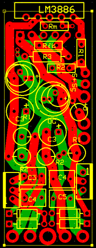
1 inch wide, 2.65 inches long.
better?
The only thing I don't like about it is that the low level input is right near the high level output. And the power traces are a bit longer.
Hi cjd,
For rabstg's purpose the inverting topology doesn't seem too useful.
Also, I'd consider the supply and output traces too narrow and, as you mention, too close to the input circuitry. They might introduce noise/hum or cause oscillation without proper bypassing and input- and output-filtering.
Hope this helps,
Sebastian.
better?
The only thing I don't like about it is that the low level input is right near the high level output. And the power traces are a bit longer.
For rabstg's purpose the inverting topology doesn't seem too useful.
Also, I'd consider the supply and output traces too narrow and, as you mention, too close to the input circuitry. They might introduce noise/hum or cause oscillation without proper bypassing and input- and output-filtering.
Hope this helps,
Sebastian.
Yep, you're right. Sorry, I misunderstood you in a former post when you said the following:
As for the trace widths, I'm not so much talking about absolute thickness. But they seem too close to each other at some points, and - as you already mentioned yourself - seem too close to the small signal circuitry. My point basically is: changing this will certainly lead to too small traces. Also, how would the regulators be cooled in your arrangement (e.g. they could be bolted to a heatsink underneath the board)?
I'm not telling you that it won't work the way it is, though!
Sebastian.
PS: As one can see in my project I pointed to in a former post, I would highly recommend SMT components at this point. The integration that is required in this thread requires a very large portion of the board area for copper traces (and thus very small components), as the reduction in board space doesn't lift the physical requirements on the current that flows through the copper traces.
I have an inverted chip-amp layout that'll sit in place of the NI layout with all the inputs/outputs in exactly the same spots.
As for the trace widths, I'm not so much talking about absolute thickness. But they seem too close to each other at some points, and - as you already mentioned yourself - seem too close to the small signal circuitry. My point basically is: changing this will certainly lead to too small traces. Also, how would the regulators be cooled in your arrangement (e.g. they could be bolted to a heatsink underneath the board)?
I'm not telling you that it won't work the way it is, though!
Sebastian.
PS: As one can see in my project I pointed to in a former post, I would highly recommend SMT components at this point. The integration that is required in this thread requires a very large portion of the board area for copper traces (and thus very small components), as the reduction in board space doesn't lift the physical requirements on the current that flows through the copper traces.
Ahh - I understand your confusion on the inverted bit. Somewhere a while ago I put together IGC and NIGC boards to go with a regulated power supply that were an inch by an inch and a little (don't recall exactly how big). The inputs, power, and outputs all lined up between the two, which means tossing the regulator portion to an inverted setup would be simple. Just was an option, and if it ever goes bridge-parallel it may be a worthwhile and needed option.
I'm not convinced that a board with the chip on the narrow end makes any sense at all, for a lot of reasons. As you noted, the regs in this case still need some heat-sink, and if you put a HS on the side, why not put the chip on the side then?! You're probably right about SMT as well - this was a quick "can I do this" try more than anything. I'll only ever make the previous layout I posted, which puts the chip to one side and keeps the traces further apart. And that one hasn't been given all that much consideration yet, as far as making sure it won't cause any problems (such as those you mentioned regarding this recent one).
I suspect there may be some trouble on the regulator portion with respect to traces being too close together. Which may mean I just need to make it a bit wider, or find a different solution.
By the time I get around to making more amps, I may just go P2P for a rats nest of beauty, and one heck of a miserable mess to root through if I ever need to troubleshoot. Not that I'd need to do that.
C
Somewhere a while ago I put together IGC and NIGC boards to go with a regulated power supply that were an inch by an inch and a little (don't recall exactly how big). The inputs, power, and outputs all lined up between the two, which means tossing the regulator portion to an inverted setup would be simple. Just was an option, and if it ever goes bridge-parallel it may be a worthwhile and needed option. I'm not convinced that a board with the chip on the narrow end makes any sense at all, for a lot of reasons. As you noted, the regs in this case still need some heat-sink, and if you put a HS on the side, why not put the chip on the side then?! You're probably right about SMT as well - this was a quick "can I do this" try more than anything. I'll only ever make the previous layout I posted, which puts the chip to one side and keeps the traces further apart. And that one hasn't been given all that much consideration yet, as far as making sure it won't cause any problems (such as those you mentioned regarding this recent one).
I suspect there may be some trouble on the regulator portion with respect to traces being too close together. Which may mean I just need to make it a bit wider, or find a different solution.
By the time I get around to making more amps, I may just go P2P for a rats nest of beauty, and one heck of a miserable mess to root through if I ever need to troubleshoot. Not that I'd need to do that.
C
- Status
- This old topic is closed. If you want to reopen this topic, contact a moderator using the "Report Post" button.
- Home
- Amplifiers
- Chip Amps
- Another LM3886 PCB!!