I'm trying to built the amplifier I found at http://www.irf.com/technical-info/appnotes/an-948.pdf
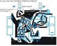
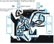
In fact I've built it, but some things are missing, because the PCB is not very clear. I've attached the PCB with the components drawn on it. Can you tell me if it is correct? If it needs something more?
In fact I've built it, but some things are missing, because the PCB is not very clear. I've attached the PCB with the components drawn on it. Can you tell me if it is correct? If it needs something more?
Attachments
That was not a design from an audio engineer, the boad layout leaves a lot to be desired.
The gate of Q6 needs to go through a resistor (try 220R) to the collector of Q4, the drain goes to the negative rail voltage.
Q3 must be attached to the heatsink, and have a cap across CE on the board (0.1µF~10µF).
C2 needs a 0.1µF in parallel, as does C3.
Q1, Q2 are in wrong, depends on the pin-out of the devices used, but they are wrong in any event.
Considering that this may be your first project, I would choose something different, this would be too much of a challenge.
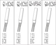
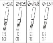
Sorry, I forgot to mention that I have replaced Q1, Q2, Q3, Q4.
Q1=BC640 Q2=BC560 Q3=MPSA43 Q4=BC549.
I have built quite a lot of other projects. It's just that this one, even though DOES have a PCB layout BUT is not very clear and some things (like bridges(I mean wires from one point to another)) are missing.
I have attached the layout of the transistors.
Q1=BC640 Q2=BC560 Q3=MPSA43 Q4=BC549.
I have built quite a lot of other projects. It's just that this one, even though DOES have a PCB layout BUT is not very clear and some things (like bridges(I mean wires from one point to another)) are missing.
I have attached the layout of the transistors.
Attachments
You clearly have either Q1 or Q2 in backwards. The basic IRF design is poor, so is their board layout.
The grounding scheme stinks. As a bare minimum, cut the trace on R1, C1, R7 away from ground, and add 10 ohms between the two. Drill a pair of holes near R15, one for power ground, the other for the speaker ground.
You will need clamp diodes on the outputs, and a gate resistor on Q6, probably some compensation on Q4 as well. L1 needs a damping resistor.
I would rather adapt the $6 A40 board:
http://www.audioxpress.com/bksprods/pcbs/nelsonpass.htm
http://www.passdiy.com/pdf/a40.pdf
hi aetosa,
I had a quick look at your eagle files, and, althougn I'm not an expert, I would like to add a word of caution. You need to carefully check all the small signal transistor pins.
Also, Q1 should be the same as Q2 and the output devices on the PCBs usually have the heatsink facing the edge of the board.")
good luck
I had a quick look at your eagle files, and, althougn I'm not an expert, I would like to add a word of caution. You need to carefully check all the small signal transistor pins.
Also, Q1 should be the same as Q2 and the output devices on the PCBs usually have the heatsink facing the edge of the board.
good luck
I have checked the small signal transistor pins lots of times, and haven't found anything...
I also thought that Q1 should be the same as Q2, BUT, in the app note
http://www.irf.com/technical-info/appnotes/an-948.pdf
is written : 'Q1 , Q2 , 2N4356, 2N5086'
From which I understood that:
Q1=2N4356 (I've put equivalent BC640)
Q2=2N5086 (I've put equivalent BC560)
In the real PCB, I've put the output devices (I think you mean Q5 & Q6) with their Heatsinks facing the edge of the board.
 , but I have learnt a lesson.
 - Status
- This old topic is closed. If you want to reopen this topic, contact a moderator using the "Report Post" button.
- Home
- Amplifiers
- Solid State
- AN948 amp project