Sounds like a good plan. It should be included as a package with the PCB though
! agree!
The red clipping LED too. That is the same LED used in NwAvGuy's O2 which is discontinued now, but I have big bunch of them here. All the other parts should be current stock at Mouser.For an alternative to the FET-input dual LME49880 I would suggest the NJR FET-input dual MUSES 8920, which is part number 513-MUSES8920E at Mouser for $11.70. The MUSES line is supposed to be the high-end audio version of the NJM2068 used in NwAvGuy's O2 headamp. The pinout is the same and it should just drop right in. I haven't tried one in the board yet, but I have a bunch here and will on a second board build-up.
MUSES 8920 data sheet: http://www.njr.com/semicon/PDF/MUSES8920_E.pdf (opens PDF)
Mouser page: MUSES8920E NJR | Mouser
Here is a possible point of confusion. NJR also has a DIP version, the MUSES 01, that goes for $46: Mouser part #513-MUSES01. This 8920 is the SMD part for $11.70. According to the NJR marketing literature (lol!) the DIP part is the individually laser-trimmed "audiophile" part, while the SMD version is the "mass production" part. My guess is the DIP part is just $30 of "added dealer profit", but I have no proof - or quantitative measurements - of that.
Last edited:
Congratulations!!
I can attest this version of the amp really works very well and sounds great.
Cant wait to put one together!!
Alex
Thanks!
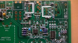
The six spare boards I had from the fabrication run have all been sold already. The Gerber files to have your own PC boards made are posted out on the Google Drive link now, but in case something happens to that over time I'm going to post the Gerber files below.
The specifications you need to give the fab:
* dimensions are 124.5mm x 80.0mm
* 4 layer
* 1.6mm board
* 1 oz copper
The specifications you need to give the fab:
* dimensions are 124.5mm x 80.0mm
* 4 layer
* 1.6mm board
* 1 oz copper
Attachments
Wow! That was fast...
Congrats on the folks that got these boards you in for a real treat ....having listened to one for a few days its really a special one of a kind design that not many people will have the pleasure of listening to!
I am looking forward to building one soon as well!!
Merry Christmas to all!
Alex
Congrats on the folks that got these boards you in for a real treat ....having listened to one for a few days its really a special one of a kind design that not many people will have the pleasure of listening to!
I am looking forward to building one soon as well!!
Merry Christmas to all!
Alex
Hey Alex! The interest surprised me too. All folks who had built some of my other projects here and emailed me.
I've sent another small run of 10 boards in for fabrication a few days ago. Exactly the same V3.6 since I've tested it. No changes. They should be back by January 3 with any luck. If anyone else is interested in a board please send me a PM or email. Same thing, at-cost at $16 plus actual shipping cost for anyone registered here on the forum. The $16 will include the red clipping led (its the one from NwAvGuy's O2 that isn't made anymore).
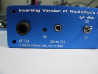
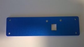
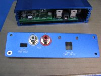
I received the first V1.0 test rear panel today from Front Panel Express. The panel is not-exactly-a-success, which I was kind of expecting. Somehow I managed to align the power jack perfectly left and right but missed by a mile vertically. Back to the math on that one. The 15.5mm insulators on those two vertical Rean RCA jacks don't quite make it either. They overlap each other by 1mm between the jacks and hit the top and bottom of the case by about 0.5mm. Well that is why we test these things.
So... as luck would have it, now that I've abandoned the batteries, the two RCA jacks appear to fit just fine on the rear panel space above the ODAC board, to the right of the USB connector. Room to spare in all dimensions. Here goes V2.0 out to FPE.
I'm in and out for the holidays over the next week. It may take a few days before I see a PM or check email and reply. Happy holidays!!
All folks who had built some of my other projects here and emailed me.I've sent another small run of 10 boards in for fabrication a few days ago. Exactly the same V3.6 since I've tested it. No changes. They should be back by January 3 with any luck. If anyone else is interested in a board please send me a PM or email. Same thing, at-cost at $16 plus actual shipping cost for anyone registered here on the forum. The $16 will include the red clipping led (its the one from NwAvGuy's O2 that isn't made anymore).
I received the first V1.0 test rear panel today from Front Panel Express. The panel is not-exactly-a-success, which I was kind of expecting. Somehow I managed to align the power jack perfectly left and right but missed by a mile vertically. Back to the math on that one. The 15.5mm insulators on those two vertical Rean RCA jacks don't quite make it either. They overlap each other by 1mm between the jacks and hit the top and bottom of the case by about 0.5mm. Well that is why we test these things.
So... as luck would have it, now that I've abandoned the batteries, the two RCA jacks appear to fit just fine on the rear panel space above the ODAC board, to the right of the USB connector. Room to spare in all dimensions. Here goes V2.0 out to FPE.
I'm in and out for the holidays over the next week. It may take a few days before I see a PM or check email and reply. Happy holidays!!
Last edited:
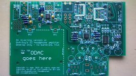
Front panel FPE CAD posted + ODAC wiring
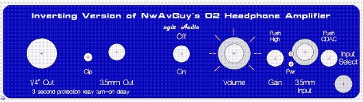
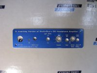
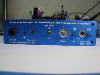
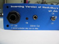
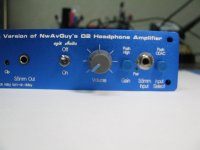
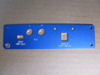
I've received the front panel for this project back from Front Panel Express today and... the thing is 99% correct on the first try. The holes are all perfect. I just forgot the countersinking around the bottom right mounting hole to electrically connect the panel to the case. That in turn requires the text for the input select to move. Both of those are fixed now.
I've posted the final FPE CAD file (.fpd) out on the project Google Drive link and included in the zip file below, along with a JPEG image of the panel. Also attached is the FPE submission instructions on how to submit the file and where to mail your blank panel(s) from the B5-080 case to Front Panel Express. The CAD file is set up for mailing in the blanks, ie no corner mounting holes since those are pre-drilled in the blank. The CAD file is done in blue, but since it is set up for "customer provided material" that doesn't mattter. The panel will be whatever color blank you mail in.
The panel is set up for white fill on the text. If you are sending in some other color panel you may wish to change that. They offer a dozen or so colors. In their Front Panel Desiger Program (free download, you will need it to submit the file, full instruction in the included README file) just right click on each bit of text, then click on the fill colors. If you chose "no fill", which is just the bare aluminum showing through, that will save $8 or so. Otherwise the panel prices up in their program at around $48 dollars plus the $5 shipping.
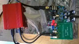
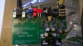
ODAC wiring
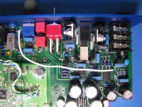
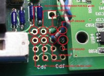
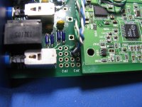
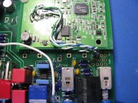
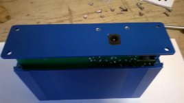
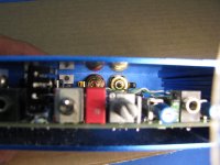
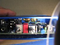
Below I've also attached some photos showing how the ODAC wires into V3.6. I've included a second row of ground holes and signal pass-through holes to make wiring up the rear RCA jacks easy. In this case you can see in the photo what the top traces do by jumpering the left and right signal inputs from the ODAC on to a second set of holes that you can use to feed the rear RCA jacks. The two rows of ground PDB holes are all connected together, of course.
If using the rear RCA jacks for ODAC outs you should run a twisted pair of ground/signal out to each RCA jack, same as the twisted pair in the photo coming from the ODAC. The rear RCA jacks are insulated from the panel, which keeps the input and output ground star segments intact.
The long white wire in the photos that goes from a PCB hole near the volume pot to a hole near the 14 pin chip is a sense wire for the clipping detect circuit. The output section was close enough to use a PC trace but for sensing the input section the distance was long enough I just used a jumper wire. See the build instructions.
I've received the front panel for this project back from Front Panel Express today and... the thing is 99% correct on the first try.
The holes are all perfect. I just forgot the countersinking around the bottom right mounting hole to electrically connect the panel to the case. That in turn requires the text for the input select to move. Both of those are fixed now.I've posted the final FPE CAD file (.fpd) out on the project Google Drive link and included in the zip file below, along with a JPEG image of the panel. Also attached is the FPE submission instructions on how to submit the file and where to mail your blank panel(s) from the B5-080 case to Front Panel Express. The CAD file is set up for mailing in the blanks, ie no corner mounting holes since those are pre-drilled in the blank. The CAD file is done in blue, but since it is set up for "customer provided material" that doesn't mattter. The panel will be whatever color blank you mail in.
The panel is set up for white fill on the text. If you are sending in some other color panel you may wish to change that. They offer a dozen or so colors. In their Front Panel Desiger Program (free download, you will need it to submit the file, full instruction in the included README file) just right click on each bit of text, then click on the fill colors. If you chose "no fill", which is just the bare aluminum showing through, that will save $8 or so. Otherwise the panel prices up in their program at around $48 dollars plus the $5 shipping.
ODAC wiring
Below I've also attached some photos showing how the ODAC wires into V3.6. I've included a second row of ground holes and signal pass-through holes to make wiring up the rear RCA jacks easy. In this case you can see in the photo what the top traces do by jumpering the left and right signal inputs from the ODAC on to a second set of holes that you can use to feed the rear RCA jacks. The two rows of ground PDB holes are all connected together, of course.
If using the rear RCA jacks for ODAC outs you should run a twisted pair of ground/signal out to each RCA jack, same as the twisted pair in the photo coming from the ODAC. The rear RCA jacks are insulated from the panel, which keeps the input and output ground star segments intact.
The long white wire in the photos that goes from a PCB hole near the volume pot to a hole near the 14 pin chip is a sense wire for the clipping detect circuit. The output section was close enough to use a PC trace but for sensing the input section the distance was long enough I just used a jumper wire.
See the build instructions.Attachments
-
 front 6.JPG252.4 KB · Views: 260
 -
inverting O2 front panel CAD for FPE.zip12.4 KB · Views: 39
-
 IMG_3884.JPG705.3 KB · Views: 102
 -
 source PCB wiring.jpg179.3 KB · Views: 244
 -
 IMG_3883.JPG619.2 KB · Views: 242
 -
 IMG_3882.JPG730.6 KB · Views: 248
 -
 IMG_3885.JPG723.8 KB · Views: 259
 -
 IMG_3874.JPG522.7 KB · Views: 100
 -
 IMG_3875.JPG586.4 KB · Views: 101
Last edited:
panel photos part 2
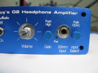
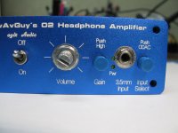
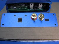
Here are some photos of the panel (post above) in place.
* The first three are without any of the jack nuts installed, but I do have blue caps on the two push button switches. C&K makes black, red, white and blue button caps (Mouser, Digikey). The "input select" lettering is now out to the right of the hole in the posted CAD file, with the bottom right mounting hole now countersunk.
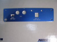
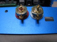
* The 4th photo is with the nuts installed on the 3.5mm input jack and washer & nut on the pot. Both are countersunk to break the annodization, allowing electrical contact. The input jack is the single ground point for the case. The pot just grounds the shaft, which prevents hand capacitance from getting into the audio. The 3.5mm jack nut clears that hole for the top power LED just fine.
* The 5th photo is with the nut installed on the 1/4" jack. Note the 3.5mm output jack has the plastic around teh nose now to insulate it from the panel.
* The final photo is with the knob on the volume pot.
Here is one thing to keep in mind when installing the nuts. The pot and the 3 jacks don't come all the way up to the panel in back. There is about a 1mm space. In the case of the 3.5mm jacks, that is just as far as they can physically go forward since they have a ground PCB lead in right at the front of the jack. In the case of the 1/4" output jack there is a ground point sticking out which is designed to dig into whatever is in front of the jack. I don't want it contacting the panel (again keeping the input and output ground star separate). So just finger-tighten the jack and pot nuts initially until you get the 4 front panel-to-case screws installed. Then go back and tighten the jack and pot nuts. The second photo in post $46 above shows the small spacing between the jacks and panel in the back.
Here are some photos of the panel (post above) in place.
* The first three are without any of the jack nuts installed, but I do have blue caps on the two push button switches. C&K makes black, red, white and blue button caps (Mouser, Digikey). The "input select" lettering is now out to the right of the hole in the posted CAD file, with the bottom right mounting hole now countersunk.
* The 4th photo is with the nuts installed on the 3.5mm input jack and washer & nut on the pot. Both are countersunk to break the annodization, allowing electrical contact. The input jack is the single ground point for the case. The pot just grounds the shaft, which prevents hand capacitance from getting into the audio. The 3.5mm jack nut clears that hole for the top power LED just fine.
* The 5th photo is with the nut installed on the 1/4" jack. Note the 3.5mm output jack has the plastic around teh nose now to insulate it from the panel.
* The final photo is with the knob on the volume pot.
Here is one thing to keep in mind when installing the nuts. The pot and the 3 jacks don't come all the way up to the panel in back. There is about a 1mm space. In the case of the 3.5mm jacks, that is just as far as they can physically go forward since they have a ground PCB lead in right at the front of the jack. In the case of the 1/4" output jack there is a ground point sticking out which is designed to dig into whatever is in front of the jack. I don't want it contacting the panel (again keeping the input and output ground star separate). So just finger-tighten the jack and pot nuts initially until you get the 4 front panel-to-case screws installed. Then go back and tighten the jack and pot nuts. The second photo in post $46 above shows the small spacing between the jacks and panel in the back.
Attachments
Last edited:
Hey Nice Panel!!
I think I am going to have to spring for one!!!!
FYI...I have completed my version of this amp this New Years Day! I had one diode D3, in backwards that caused me some concern...the one in between the WIMA caps....had to remove the forward WIMA to get to the diode to carefully remove it, It was a real bugger to get out...the leads fit in real snug and solder wick doenst do a great job here...but with a little of perserverance and a little flux added to the wick we were able to wiggle it out and check!
It checked out ok, reinstall "correctly" and voila both power rail leds on and no DC volts present ....then 'music" !!
Its indeed "alive!!!'
More later
Alex
Ok here are some of my build pictures...AGDR kindly installed the SMD caps on the backside of the PC board as well as the three SMD IC's on the top side.
Important to measure your resistors and make sure you dont get them mixed up, as well as the diodes!!!!!
The Buffers have pretty close holes and be careful not to bridge these when soldering them in.
I would advise to check and re-check the bottom side for errant solder blobs and any shorts. It can ruin your day!
Its a great feeling to hear something you have spent hours on....and I cant thank AGDR enough for carrying the O2 torch and coming up with these improvements !!!
I hope the guys who got these boards assemble and post your impressions!
Mine are awesome, its a very neat, special design and not many people will ever hear it, unless.....
Back to listening and need to order a case!
Attachments
Alex - congratulations on your build! Looks great.
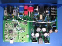
I can't remember if I've posted this yet or not, but it turns out there is no need at all to install those two battery terminals to mechanically backstop the ODAC. NwAvGuy only put one hole in the O2 PCB for the ODAC, as I recall, but I went ahead and put in all three. In those photos I posted above (post #46) of the ODAC isntallation I inserted a second nylon bolt in front. Works perfectly. Those photos use actual 3mm metric bolts (I bought some longer 8mm nylon bolts on eBay). Turns out the metric nuts are just the perfect size for spacing between the ODAC and inverting O2 board. The board winds up perfectly flat when inserted in the second slot up. So 3mm bolt up through the bottom of the PC board, then a 3mm nut, then the ODAC, then another 3mm nut.
Looks great.I can't remember if I've posted this yet or not, but it turns out there is no need at all to install those two battery terminals to mechanically backstop the ODAC. NwAvGuy only put one hole in the O2 PCB for the ODAC, as I recall, but I went ahead and put in all three. In those photos I posted above (post #46) of the ODAC isntallation I inserted a second nylon bolt in front. Works perfectly. Those photos use actual 3mm metric bolts (I bought some longer 8mm nylon bolts on eBay). Turns out the metric nuts are just the perfect size for spacing between the ODAC and inverting O2 board. The board winds up perfectly flat when inserted in the second slot up. So 3mm bolt up through the bottom of the PC board, then a 3mm nut, then the ODAC, then another 3mm nut.
Last edited:
V3.61 - two small errors found in V3.6
A big thanks goes out to a poster on Head-Fi who spotted a couple of part problems on the schematic! The existing version 3.6 PC board still works just fine with these changes:
* The two reference zeners for the clipping detect circuit, D7 & D8, are backwards. The folks building this amp right now just need to insert these diodes with the band opposite from the board marking. If you have them in backward right now it won't blow anything up, the clipping detect levels just won't be correct until they are reversed.
* Two of the capacitors symbols on the schematic are upside down, C37 and C39. Luckily these are not polarized capacitors, one is film and the other is ceramic, so it doesn't matter how you have them installed. For some reason the Eagle standard library uses a simlar symbol for polarized and non-polarized capacitors, they just add a "+" on the polarized ones. Ideally the symbol really shouldn't be directional in any way for the non-polarized caps. In the future I might make some of my own "straight plate" symbols for the non-polarized.
* I should be saying the maximum gain of the output stage is 1.33x, since the "ac" gain of that stage will vary with the volume pot. This is different than NwAvGuy's O2 and is a by-product of the way inverting stages work. The "dc" gain of the stage is a fixed 1.33x. The gain of the output stage will actually vary from 1.1x to 1.33x, depending on volume control position. The amount of variation is small because the volume pot is small (5K) relative to the other series stage input resistor (24.9K).
I've fixed these issues these issue in a new V3.61 which is now also out on the Google Drive link for the project, and posted below. I've re-generated a set of gerber files for V3.61 and posted those too.
In addition to the above issues, I've made a few more changes in V3.61. These are all minor and don't affect performance. None is major enough to warrant another board turn:
* There are now 3 "set" resistors for the LT3080 rather than two. Two larger 0.1% 1/4W size (1 meg and 500K) and one 1/8W-sized 30K. The issue here is that the LT3080 works by putting a very small (10uA) current through the "set" resistors, which then wind up being large values, 1.5meg (+30K) in this case. Having these resistors accurate is important to exactly hit the desired voltage target, but 1.5meg resistors are not available in 0.1% in through-hole from Mouser. On my first build with 1% 1.5meg and 30K I wound up with 1.55Vdc on the positive rail due to tolerance in that 1.5 meg, vs. -15.29 on the negative rail (which is a good match for the -15.3V target). I had to reduce the 30K to 2K to hit +15.29, to compensate for the 1.5meg variation. Splitting the 1.5 meg up into series 1 meg and 500K allows using 0.1% resistors.
* related to the above, I've added a datasheet-recommended guard ring around the "set" parts, with the ring tied to the output voltage. The set current is so small at 10uA that it is possible to get PC board bleed without a guard ring.
* I've removed the battery terminals, since they are not needed any more. I've verified that installing a nylon bolt in a second ODAC hole is enough to secure it.
* related to the above, removing the battery terminals freed up space to move the hole for the clipping circuit jumper wire, JP10, down to that area, shortening that wire.
I've also just discovered an interesting passage in NwAvGuy's O2 blog. In the "O2 design process" blog here
NwAvGuy: O2 Design Process
where he discusses the volume control being in the middle, in section 2-11 he says:
“See 2-3 above for why the volume control is best positioned between the two stages rather than before the input/gain stage. The main downside to the “volume control in the middle” approach is it’s easier to overload the gain stage which always runs wide open. The O2 has a gain switch to address this problem but it’s something those altering the default gain settings should be aware of. See: Gain Stage Overload. A compromise is a “split gain” design where you divide up the gain between two sections but this requires the output stage, in a 2 stage amp, be capable of gain (many buffers are not) and usually requires additional components taking up board space.”
Well the inverting version here IS a split-gain design, with the input and output stages each having gain. Just like he says that lowers the maximum gain of the input stage, which further helps prevent clipping along with the extra 3V headroom of the +/-15.3Vdc power supplies. In this case, of course, the amp has a clipping detector to solve the problem he mentions of clipping a stage and not being aware of it. Great suggestion early in this thread to add that from sgrossklass!
Attachments
-
Inverting O2 PCB BOM V3.61 2.zip25.3 KB · Views: 58
-
Inverting O2 V3.61 1_5_2016.zip333.3 KB · Views: 61
-
 layer 4 ground.jpg983.7 KB · Views: 71
 -
 layer 3 V+.jpg986.2 KB · Views: 297
 -
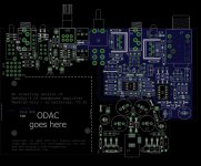 layer 2 V-.jpg996.2 KB · Views: 310
 -
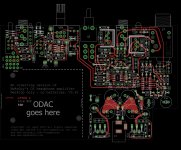 layer 1 top.jpg971.9 KB · Views: 328
 -
layout.pdf488.2 KB · Views: 81
-
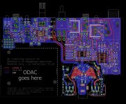 layout.jpg990.7 KB · Views: 341
 -
schematic.pdf62.7 KB · Views: 81
-
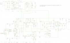 schematic.jpg631.4 KB · Views: 343
Last edited:
I finished my inverting O2 amp and am in the process of getting onto a case. I sent a panel to Panel Express and am waiting on them to complete the panel and engraving. I will post pictures when I get it. I elected to have the engraving done with no paint or xolor fill. It brought the cost down to $35.10. Shipping back will be approx $5..so a total of $40 for a nice front panel.
For the rear I elected to drill the two holes for the buffers to the rear panel acting as the heatsink. I also drilled and filed out the square hole for the AC power jack.
The rear panel is not as complicated or busy as the front and is easily done by a DIY if you have a steady hand, a drill press and some good sharp files.
I Mounted the heatsinks to the buffers for stand alone operation and used these as hole locators....I fasten the back panel to the enclosure, then apply some black paint to the srcews that hold the heatsink on and slide the pc board into the enclosure slowly and the screws touch the rear panel and the paint leaves a nice round spot. I let it dry and use a center punch to locate the center of the hole and them drill it out...voila!
The AC jack on the pc board is done the same way...use some black paint (u can use craft paint, the testors model airplane paint or even white out)....the AC jack leaves a nice square outline of where the hole needs to be.
Here are a few pix. I will post more when I get the mounting hardware. The buffer heatsinks are removed and not used but remember to use a mica washer and nylon shoulder sleeve insert to electrically isolate the buffers from the case. AGDR has all this updated in the build instructions.
Alex
Attachments
Rear panel is back and works! FPE CAD posted
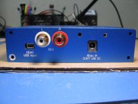
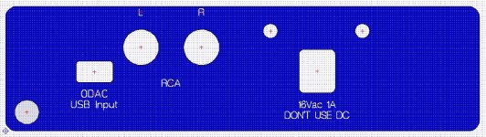
I received try #2 on the inverting O2 rear panel from Front Panel Express today and it works! The RCA jacks above the ODAC board worked out fine. The spacings are exactly as expected.
The FPE file posted below is assuming you are sending in the blank rear panel that comes with the B5-080 case, since the blank has pre-drilled corner mounting holes.
The panel fits fine, but I've made 3 small changes in the posted file below just to insure good fits if the parts on the board are moved around slightly during soldering. I'ved added 0.2mm to the height and width of the AC power jack hole, increased the ODAC USB port hole height to 6mm from 5.5mm, and moved the "L" and "R" labels for the RCA jacks down 0.1mm.
* The first two photos are the panel from FPE, on and off the shrink-wrap.
* The next 3 photos show mounting the insulated Rean RCA jacks on the panel. The order to assemble here is jack - washer - panel - washer - nut 1 - ground lug - nut 2. The ground lugs can't hang down like I show in the 2nd & 3rd photo or they hit the ODAC board. I found that out when I tried the panel on the case the first time. The have to be moved out to the side, as in the 6th and 7th photos below that look into the case. Plenty of clearance when they are oriented off to the side.
* The next 2 are just verifying clearances from the jack's washer to the top of the case and top of the ODAC board. All worked out fine.
* and finally the panel sitting in place on the back of the case. The USB jack and AC jack are lined up just fine left-to-right in their holes. The angle of the camera here is what's making it look like the USB jack is off to one side.
I'm going to post another round of pictures when I get the RCA jacks wired in, to show how that works, and the voltage regulators mounted with the mica and nylon washers. I'll take some dead-on shots of the USB and AC jack holes then to show alignment.
I received try #2 on the inverting O2 rear panel from Front Panel Express today and it works! The RCA jacks above the ODAC board worked out fine. The spacings are exactly as expected.
The FPE file posted below is assuming you are sending in the blank rear panel that comes with the B5-080 case, since the blank has pre-drilled corner mounting holes.
The panel fits fine, but I've made 3 small changes in the posted file below just to insure good fits if the parts on the board are moved around slightly during soldering. I'ved added 0.2mm to the height and width of the AC power jack hole, increased the ODAC USB port hole height to 6mm from 5.5mm, and moved the "L" and "R" labels for the RCA jacks down 0.1mm.
* The first two photos are the panel from FPE, on and off the shrink-wrap.
* The next 3 photos show mounting the insulated Rean RCA jacks on the panel. The order to assemble here is jack - washer - panel - washer - nut 1 - ground lug - nut 2. The ground lugs can't hang down like I show in the 2nd & 3rd photo or they hit the ODAC board. I found that out when I tried the panel on the case the first time.
The have to be moved out to the side, as in the 6th and 7th photos below that look into the case. Plenty of clearance when they are oriented off to the side.* The next 2 are just verifying clearances from the jack's washer to the top of the case and top of the ODAC board. All worked out fine.
* and finally the panel sitting in place on the back of the case. The USB jack and AC jack are lined up just fine left-to-right in their holes. The angle of the camera here is what's making it look like the USB jack is off to one side.
I'm going to post another round of pictures when I get the RCA jacks wired in, to show how that works, and the voltage regulators mounted with the mica and nylon washers. I'll take some dead-on shots of the USB and AC jack holes then to show alignment.
Attachments
-
 IMG_3975.JPG631.7 KB · Views: 69
 -
 IMG_3974.JPG564.1 KB · Views: 72
 -
Inverting O2 rear panel 8 send blank.zip737 bytes · Views: 39
-
 IMG_3977.JPG657.2 KB · Views: 66
 -
 IMG_3978.JPG644.9 KB · Views: 73
 -
 IMG_3979.JPG750.1 KB · Views: 67
 -
 IMG_3980.JPG527.3 KB · Views: 70
 -
 IMG_3981.JPG528.5 KB · Views: 75
 -
 IMG_3983.JPG548.3 KB · Views: 80
 -
 rear panel 8.JPG246.9 KB · Views: 78
Last edited:
- Status
- This old topic is closed. If you want to reopen this topic, contact a moderator using the "Report Post" button.
- Home
- Amplifiers
- Headphone Systems
- An inverting version of the NwAvGuy O2 headphone amp vs. the original: THD+N