"In my self taught world of electronics I have the idea that it's good to follow a device with high o/p impedance ( like a current mirror or indeed a cascode ) on an i/p stage, for instance, with a device with an even higher i/p impedance i.e. a mosfet."
Sure, that's why people add emitter followers between diff amp and VAS, and between VAS and output stages, so as to minimize the loading effect.
Sure, that's why people add emitter followers between diff amp and VAS, and between VAS and output stages, so as to minimize the loading effect.
LukasLouw said:Sure, that's why people add emitter followers between diff amp and VAS, and between VAS and output stages, so as to minimize the loading effect.
that's interesting, I was not aware of that practice. Would this prevelant in amps with low or no overall feedback? Otherwise I'm not sure what advantages would be over a well designed high gain, fast, simple three stage cct.
do you know of an example that uses this kind of technique that you could point me towards.
god this is like being back in school
thanks
mike
Collector loading of diff amp and other things...
Eric,
I'm not sure about the distortion effects of the input cascode actually. My gut feeling (and it's only that) is that it should have little effect. My response to Lukas was unclear. I was mainly concerned about the collector loading of the cascoded diff amp compared to the non-cascoded version. This can affect the input capacitance of the amp. I thought that if Dave S's amp had an input low pass filter with a fairly large series resistor and small input capacitor that reducing the input capacitance of the amp would have the effect of increasing that filter's cutoff frequency. This could possibly affect its susceptibility to RFI and/or TIM distortion and thus its sound.
Let's look at the impedance at the collector of the input diff amp of the complementary amplifier, since both Jan and P-A have brought this issue up previously as well. After responding to Dave S about input capacitance, I then changed my mind, thinking that the collector load impedance seen by the diff amp at high frequencies would actually be lower in the conventional configuration than the cascode configuration. I reasoned that since this impedance establishes the dominant open-loop pole, that said impedance would be very low at the input low-pass filter cutoff frequency (probably a hundred kHz or so). While the collector load impedance does establish the dominant pole, there is also a zero in that impedance which causes the impedance to approach a constant value as the frequency becomes large. That constant value turns out to be much larger than the load that a cascode would place on it. So I was right the first time and wrong the second.
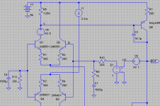
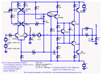
Let me clarify how this zero comes about. Below I've shown the original complementary design with a couple of new nodes labeled. I've grounded the input for AC, and placed the node label "B" on the base of the diff amp that's inside the feedback loop, and the label "C" on the collector that drives the Miller integrator. There's a voltage source in that collector whose value is zero. It's there only to probe its current as I(V5) so I can compute the impedance. There's also a node labeled "OUT" at the output. Excitation is at the floating source V4 in the feedback loop connected to the output. Let's look at the open loop voltage gain of the amp as a whole, and the open-loop gains of the diff amp and VAS. Finally I'll look at the collector load impedance. More to come...
capslock said:
Lukas, Andy,
this beats me, can you explain some more? Of course, the cascode on the LTP increases its output impedance, thereby increasing gain, if only a little because of the low input impedance of the following VAS input. But why would this result in increased distortion??
Eric,
I'm not sure about the distortion effects of the input cascode actually. My gut feeling (and it's only that) is that it should have little effect. My response to Lukas was unclear. I was mainly concerned about the collector loading of the cascoded diff amp compared to the non-cascoded version. This can affect the input capacitance of the amp. I thought that if Dave S's amp had an input low pass filter with a fairly large series resistor and small input capacitor that reducing the input capacitance of the amp would have the effect of increasing that filter's cutoff frequency. This could possibly affect its susceptibility to RFI and/or TIM distortion and thus its sound.
Let's look at the impedance at the collector of the input diff amp of the complementary amplifier, since both Jan and P-A have brought this issue up previously as well. After responding to Dave S about input capacitance, I then changed my mind, thinking that the collector load impedance seen by the diff amp at high frequencies would actually be lower in the conventional configuration than the cascode configuration. I reasoned that since this impedance establishes the dominant open-loop pole, that said impedance would be very low at the input low-pass filter cutoff frequency (probably a hundred kHz or so). While the collector load impedance does establish the dominant pole, there is also a zero in that impedance which causes the impedance to approach a constant value as the frequency becomes large. That constant value turns out to be much larger than the load that a cascode would place on it. So I was right the first time and wrong the second.
Let me clarify how this zero comes about. Below I've shown the original complementary design with a couple of new nodes labeled. I've grounded the input for AC, and placed the node label "B" on the base of the diff amp that's inside the feedback loop, and the label "C" on the collector that drives the Miller integrator. There's a voltage source in that collector whose value is zero. It's there only to probe its current as I(V5) so I can compute the impedance. There's also a node labeled "OUT" at the output. Excitation is at the floating source V4 in the feedback loop connected to the output. Let's look at the open loop voltage gain of the amp as a whole, and the open-loop gains of the diff amp and VAS. Finally I'll look at the collector load impedance. More to come...
Attachments
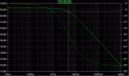
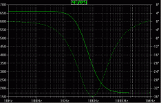
Below is the open-loop gain of the amp. Its value at DC is about 66 dB, nothing earth-shaking. Cascoding the VAS would increase this quite a bit. The dominant pole is at 4.64 kHz. We see a nice single-pole behavior out to a bit less than 1 MHz. No surprises here. Now let's see how this splits up between the diff amp and the VAS. That's when things get interesting...
Attachments
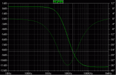
Here's the voltage gain of the diff amp. It is 3 dB down at 4.98 kHz, a little higher than the 4.64 kHz of the overall amp. That's because of the presence of the zero that's causing its gain to approach a constant at high frequencies. I've estimated the zero by finding the frequency where the gain is 3 dB higher than its asymptotic high frequency value. That's about 16.6 kHz.
Attachments
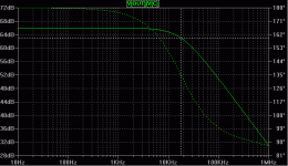
Here's the voltage gain of the VAS. Note that it has a pole, but it's not the open-loop pole of the overall amplifier! It's 3 dB down at 17.6 kHz, while the overall amp is 3 dB down at 4.64 kHz. What's happening here is that this pole is exactly canceling with the zero of the diff amp gain. Let's see how this happens. Now that we know where this pole is, we can use Miller's theorem to get an idea of the impedance seen by the input diff amp collector.
We normally use Miller's theorem to compute the input capacitance as
Cin = Ccomp * (1 - Av)
where Ccomp is the compensation capacitor and Av is the voltage gain of the VAS. However, the voltage gain is now a function of s, Av(s), with a DC gain A0 and a simple pole omegaVAS. So we need to use the more general form of Miller's theorem, in which the admittance of the capacitor is multiplied by (1 - Av(s)) to find the input admittance (taking into account that Av(0) is negative). When we do this, it becomes clear that the input admittance has a pole at the same frequency as the pole of the VAS. Therefore, the input impedance has a zero at the same frequency as the pole of the VAS. So that's where the zero of the voltage gain of the input diff amp comes from - the impedance the diff amp sees has a zero at the same frequency as the pole of the VAS. Since this zero is at the exact same frequency as the pole of the VAS, they cancel exactly, making the open-loop pole of the amplifier the same as the open-loop pole of the input diff amp voltage transfer function. Whew!
Attachments
Finally, here is the load impedance seen by the collector of the input diff amp. Note that the zero whose origin was described in my previous post causes it to approach the constant value of 173 Ohms at high frequency.
All this brings up a point I wanted to bring up earlier. Thinking about the open-loop frequency response of the amp in terms of voltage transfer functions is not the best way to approach the problem. Because of the pole-zero cancellation, it essentially takes one simple problem and splits it up into two more complex ones. On the other hand, we can think of the open-loop gain as the product of the transconductance of the diff amp and the transimpedance of the VAS. In this case, the transconductance is almost perfectly constant over frequency (not shown, I've already used up more than my share of bandwidth), and the transimpedance of the VAS has a single dominant pole. Much simpler!
So my conclusion is that if the input diff amp is cascoded, the collectors will see a load impedance of
26 mV/1.6 mA = 16.25 Ohms
which is much lower than the impedance shown below. So the input capacitance of the amplifier will be lowered by cascoding.
Attachments
"that's interesting, I was not aware of that practice. Would this prevelant in amps with low or no overall feedback? Otherwise I'm not sure what advantages would be over a well designed high gain, fast, simple three stage cct.
do you know of an example that uses this kind of technique that you could point me towards."
Mike, VAS gain enhancement is merely an emitter follower between the diff amp and teh VAS, a failry common practice. An extra current gain stage between the VAS and an output doublet is less common, I like an emitter follower with a current source there, some may use a triple darlington in teh output. All kind of configurations have been used. Examples? Self favors VAS gain enhancement. Extra current gain after teh VAS - I'm sure If I look we can find some.
Note that these are current gain stages, so the term "three stage" circuit still applies for voltage gain....
Lukas
SwCad III analysis shows highest distortion component of –136 dB with a highly asymmetric topology, 2nds higher than 3rds – I think the ridiculously low distortion levels in this example should demonstrate the futility of much of the earlier argument over the influence of symmetry on distortion, the subject is too subtle and sensitive to too many design variables for the present level of discussion/simulation to have any hope of revealing “deep truths” – read Cherry!
I started with the SwCad audioamp.asc example circuit; changing the quasi-comp output to complementary Sziklai pairs, Super Paired the VAS, current mirrored the Diff pair and added input cascodes (just to show comments about input cascodes increasing distortion to be as mistaken as anything else I’ve seen in this thread – read Hawksford too!) doubled ps V for +20 dBV output ( increased Rload, still looking good for 2N2219/2907 output Qs – sot-223 with good heat sinking could actually handle the pwr)
LT SwCad III gives higher fft res with the usual (in my Pspice experience) tweaks:
crank the tol values in the Control Panel>Spice menu ‘til it don’t work and back off a little
set max step size < 1/200 of your highest frequency in the .tran statement
Gear integration should be more accurate but more prone to numerical instability
I cleared the box to optimize accuracy in the Control Panel>Hacks menu
I’m suspicious of data file compression but didn’t see an obvious effect
don’t window fft; use a data set time = integer # of input cycles, more fft points lowers “noise” floor
use only a few ms at the end of a long .tran data set to allow t=0 transient to die out
(some of the above is likely irrelevant to maxing fft res but that’s what worked for me)
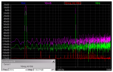
You can still see the SwCad Vin sine source has some numerical hairiness that raises the distortion floor above where we might want to be able to see. Fortunately we can “notch out” the fundamental and extend our resolution by simply looking at the differential input voltage at the amplifier’s input.
The input is 4:1 2KHz + 20KHz with a peak amplitude of 1.414 V to fool SwCad’s fft into calling it 0 dB and give us dBV. The lowest trace is the differential input voltage and the distortion component fft peak values correspond to the distortion components rms values re the input peak amplitude of the composite waveform; 2Khz input component is –2.5 dBV, 20KHz –17.5 dBV, the input signal level and distortion measured at the input are all raised by 20 dB by the amplifier’s closed loop gain of +10, leaving the distortion at the output re peak output level the same as the input referred measurement
I started with the SwCad audioamp.asc example circuit; changing the quasi-comp output to complementary Sziklai pairs, Super Paired the VAS, current mirrored the Diff pair and added input cascodes (just to show comments about input cascodes increasing distortion to be as mistaken as anything else I’ve seen in this thread – read Hawksford too!) doubled ps V for +20 dBV output ( increased Rload, still looking good for 2N2219/2907 output Qs – sot-223 with good heat sinking could actually handle the pwr)
LT SwCad III gives higher fft res with the usual (in my Pspice experience) tweaks:
crank the tol values in the Control Panel>Spice menu ‘til it don’t work and back off a little
set max step size < 1/200 of your highest frequency in the .tran statement
Gear integration should be more accurate but more prone to numerical instability
I cleared the box to optimize accuracy in the Control Panel>Hacks menu
I’m suspicious of data file compression but didn’t see an obvious effect
don’t window fft; use a data set time = integer # of input cycles, more fft points lowers “noise” floor
use only a few ms at the end of a long .tran data set to allow t=0 transient to die out
(some of the above is likely irrelevant to maxing fft res but that’s what worked for me)
You can still see the SwCad Vin sine source has some numerical hairiness that raises the distortion floor above where we might want to be able to see. Fortunately we can “notch out” the fundamental and extend our resolution by simply looking at the differential input voltage at the amplifier’s input.
The input is 4:1 2KHz + 20KHz with a peak amplitude of 1.414 V to fool SwCad’s fft into calling it 0 dB and give us dBV. The lowest trace is the differential input voltage and the distortion component fft peak values correspond to the distortion components rms values re the input peak amplitude of the composite waveform; 2Khz input component is –2.5 dBV, 20KHz –17.5 dBV, the input signal level and distortion measured at the input are all raised by 20 dB by the amplifier’s closed loop gain of +10, leaving the distortion at the output re peak output level the same as the input referred measurement
Attachments
jcx said:– read Cherry!
[...]
The input is 4:1 2KHz + 20KHz with a peak amplitude of 1.414 V to fool SwCad’s fft into calling it 0 dB and give us dBV. The lowest trace is the differential input voltage and the distortion component fft peak values correspond to the distortion components rms values re the input peak amplitude of the composite waveform; 2Khz input component is –2.5 dBV, 20KHz –17.5 dBV, the input signal level and distortion measured at the input are all raised by 20 dB by the amplifier’s closed loop gain of +10, leaving the distortion at the output re peak output level the same as the input referred measurement
Which one by Cherry? The one you recommended earlier on in this thread? Ordered those two, but JAES will snail mail them because they are not available online

Super pair: will have to do some modelling of super pair in isolation to see benefits over more conventional topologies (& wait for Hawksford). Interestingly, the super pair is not described in Tietze/Schenk, which is my bible for analog design and which has been greatly expanded one edition ago to include analog integrated circuit design. Something similar, with the collector of the first transitor connected to a current source rather than second transistor, is given as a unity gain buffer. It looks rather much like half a diamond transistor (the 4-transistor buffer you find so often in CFB op amps). Speaking of which, I wonder if a diamond transistor can be used as a VAS...
correct cascode: ok, I feel better now for not really having used incorrect cascodes so far
in a VAS with little or no emitter degeneration, it does not really matter whether the voltage is referenced to rail or emitter. And bypassing the voltage with a cap should be standard desing practice, too.Switcher CAD residuals: This seems highly interesting, but the paragraph I have quoted is Greek to me. Could you take the time to explain again what you did there?
Thanks,
Eric
cascode on LTP pair
The cascode decreases input capacitance by eliminating the Miller effect. This is beneficial, because the Miller capacitance is a function of voltage and can hence introduce common mode disto if driven from a high impedance (1-2 k as in feedback network is probably enough to make the effect visible).
As Andy pointed out, this results in less input filtering, and hence more RF dirt may get amplified. The solution is to but a bigger cap into the input filter => higher internal bandwith, less distortion, same external bandwidth.
Cascode operation is best thought of in current mode (as Andy proved with his simulations). I don't think the input transistor cares about the low collector load impedance. Actually, you arrive at this low impedance because voltage swing is limited (R=delta U / delta I), but it doesn't have much meaning.
The cascode transistor passes on the current, the only error source being its own base current. Distortion-wise, we only have to think of the change in beta over the collector current modulation we have, so this is probably less than 1/10000. I am not sure whether this is significant additional distortion.
On the other hand, the input transistor now operates at almost constant voltage, which greatly reduced the early effect and hence improves its linearity.
Greetings,
Eric
Andy C et Al - thanks for some possible explanations for the subjective effects I got with various topology changes.
In my experience implementation counts for at least as much as the circuit design. If we take cascode implementation as an example, the cascode tr. base node is in effect another input to the amplifier. A perfectly decoupled voltage reference for this node relative to a nice clean ground potential is not that easy to achieve in practise (except on a circuit simulator!). I suspect this effect outweighs any potential benefit of the cascode itself.
The other issue I have with a casode is that it adds another transistor in the signal path. The fewer transistors in the signal path the better, as far as my subjective investigations tell me (as long at the design works properly of course).
On the subjective versus objective debate I think I'm correct in stating that the AKSA was developed by a subjectivist and the Self "Blameless" amp was developed by an objectivist. The Borbely amps were developed by a very astute engineer and have a wonderfully balanced and symmetrical topology (getting a bit pervy here, I know!!. ). I cannot argue with the design decisions behind the Self and Borbely amps (actually I can but that would spoil my point) whereas I'm not wholly convinced by one or two of Hugh Dean's. However I very much prefer the sound of the ASKA's to any of the Borbely variations I tried and although I've never heard the blameless amp I have never heard any positive comments about it's music making abilities (and plenty of negative ones).
In my experience implementation counts for at least as much as the circuit design. If we take cascode implementation as an example, the cascode tr. base node is in effect another input to the amplifier. A perfectly decoupled voltage reference for this node relative to a nice clean ground potential is not that easy to achieve in practise (except on a circuit simulator!). I suspect this effect outweighs any potential benefit of the cascode itself.
The other issue I have with a casode is that it adds another transistor in the signal path. The fewer transistors in the signal path the better, as far as my subjective investigations tell me (as long at the design works properly of course).
On the subjective versus objective debate I think I'm correct in stating that the AKSA was developed by a subjectivist and the Self "Blameless" amp was developed by an objectivist. The Borbely amps were developed by a very astute engineer and have a wonderfully balanced and symmetrical topology (getting a bit pervy here, I know!!.
). I cannot argue with the design decisions behind the Self and Borbely amps (actually I can but that would spoil my point) whereas I'm not wholly convinced by one or two of Hugh Dean's. However I very much prefer the sound of the ASKA's to any of the Borbely variations I tried and although I've never heard the blameless amp I have never heard any positive comments about it's music making abilities (and plenty of negative ones)."I don't think the input transistor cares about the low collector load impedance"
Unfortunately it cares! I have no distortion meter, but we made some listening tests, with same amplifier. Just listen it, and than remove the cascode devices, and listen again. The cascode design has special distortion at the HF region. The sound will be agressive, and sharp.
But of course this is just one point of view.
Sajti
I am the subjectivist David refers to, and I've said my piece here several times. Possibly not loud enough! 
I believe most sincerely in what I have said, and will not argue the point with any of the conclusions reached by capable engineers here present, but neither will I offer precise detail about how to achieve good sound. The debate is now fiercely engineering-based, and headed in a purist direction....
I know several things about the sonics of different topologies. I have found this by building the bloody things, carefully comparing them with real music as well as the DMM and CRO, and can't speak highly enough of this approach. It is precisely what has been lacking to date in most of these arguments. Amp design in the past has led to some blindingly elegant solutions, mathematically analysed to within a picofarad of their stability, but most, it seems, sound quite ordinary, causing so many subjectivists to take flight back to a technology which dates from the beginning of last century.
A shortcoming of the engineering approach to date has been the desire to narrow things down to mathematical models, which can then be analysed in detail. Douglas Self did this with grim competence in his seminal series on amp design back in the early nineties. This leads to a circuit block mentality, where every circuit element can be quarantined neatly and thus examined in isolation. As I mentioned before in an earlier post, I am convinced that this is a 'management of compromise' situation, and that the optimum solution is probably a hybrid of several ideas. I believe we should realize that there are definite synergies in high end amplification, just as there are in auto design, architecture, computer networking, and the design of hand tools. Think a while on this situation, and understand that some of the Japanese designers, particularly tube, go to great extremes to adopt the right frame of mind before designing their amplifiers.
I trust that my launch into smug generalities is not too irritating. I have a living to make and I won't give too many of my secrets away....
Cheers,
Hugh
sajti:
A cascode device can oscillate quite easily. If there is too much physical distance between the driving voltage source and the base of the cascode transistor, the inductance of the leads can interact with the transistor capacitance to form a Collpits oscillator. Place the driving voltage source as close to the base of the cascode transistor as possible, and if any significant free lead length remains (signifying inductance), add a base stopper resistor(s).
As Dave S said, "implementation counts for at least as much as the circuit design."
hth, jonathan carr
Hugh and Jcarr make good points, and simulations can only take you so far.
Probably grist for a new thread, but I for one need a spectrum analyzer to check all these effects out in real world terms. There are not a heck of a lot of cost effective options out there. Either shell out US$25K+ for an Audio Precision Cascade, or use on of the PC sound card solutions. The soundcard solutions have their own problems with high input levels, bandwidth and calibration.
Does anyone know of USB type "soundcards" avaialble these days that are decent and will work with the spectrum analysis software out there? A USB solution will be easier to manage cabling wise, instead of having to duck behind teh PC all teh time, and I should imagine noise and interference form a PC's innardfs will be less of a problem....
Lukas
jcarr said:sajti:
A cascode device can oscillate quite easily. If there is too much physical distance between the driving voltage source and the base of the cascode transistor, the inductance of the leads can interact with the transistor capacitance to form a Collpits oscillator. Place the driving voltage source as close to the base of the cascode transistor as possible, and if any significant free lead length remains (signifying inductance), add a base stopper resistor(s).
As Dave S said, "implementation counts for at least as much as the circuit design."
hth, jonathan carr
Yes I found it. Of course we checked the amplifier with square wave, and various loads. There was no any oscillation, or ringing. The cascode transistors was very close to the input (2-3mm). When we remove them, we simply solder small wire to the empty holes to keep the signal path.
Sajti
Sajti,
I have not yet built an amp with an input cascode nor listened to it (except for a buffered OPA627 in my preamp, which does have a cascoded FET input), so I won't argue with your subjective findings.
What Jonathan means is that the base of the cascode transistor should be decoupled as close to the transistor case either to a good AC ground or (preferably?) to the emitter of the input transistor. Coming to think of it, in some transistors this near zero impedance on the base might actually invite oscillation, so a 10R resistor between cap and base might actually be a good idea.
When I built my current main amp years ago, I used a 20 MHz analog CRO at home, and was wondering about a few effects I could not explain. What a difference it was when I took the amp to work and checked with a 400 MHz scope!
And please let me stress again: thinking in terms of a resistive load on the input collector is the wrong way. Forget for a moment about LTPs and a VAS which needs current drive. Assume you have a single transistor in common emitter configuration, maybe with a little emitter degeneration. The voltage on the input makes the transistor conduct a certain current. If you have a resistor in the collector lead, the current will cause a voltage drop. As you increase the resistor, the voltage gain will increase, but the current is still almost solely determined by the input voltage. Replace the resistor with an ideal current source, and the resistance will still be final, the gain being limited by the early effect and the collector current.
Now add a cascode transistor. It will pass on 99,5% of the current if hfe=200. The voltage drop is still generated by the current, only that the resistor is now in the collector lead of the cascode transistor. The cascode transistor introduces a little bit of distortion, namely the variation of hfe with current and voltage. This is most likely offset by a huge improvement in the linearity of the input transistor that can now operate at constant voltage.
And last, not least, input capacitance becomes both smaller and more constant.
Regards,
Eric
LukasLouw said:
Does anyone know of USB type "soundcards" avaialble these days that are decent and will work with the spectrum analysis software out there? A USB solution will be easier to manage cabling wise, instead of having to duck behind teh PC all teh time, and I should imagine noise and interference form a PC's innardfs will be less of a problem....
Lukas
Try www.soundkartenkatalog.de, they have some 24 bit/96 kHz USB cards that should also be available in other countries.
Regards,
Eric
- Status
- This old topic is closed. If you want to reopen this topic, contact a moderator using the "Report Post" button.
- Home
- Amplifiers
- Solid State
- Amplifier topology subjective effects