2N3055/MJ2955 for ouput stages
MJ15030/31 for drivers
BD139/140 for predrivers
BC550C/560C for input stages and BC546B/556B for the rest of it (protections as well)
This posted schematic shows the BD139/140 as drivers, but they're really pushed hard and MJ15030/31 are better for that purpose.
MJ15030/31 for drivers
BD139/140 for predrivers
BC550C/560C for input stages and BC546B/556B for the rest of it (protections as well)
This posted schematic shows the BD139/140 as drivers, but they're really pushed hard and MJ15030/31 are better for that purpose.
In that simulation, the idling bias currents in the outputs are rather "rich", although the dissipation seems a little high for idling, it's within reason, a bit like a class A.
We can bias it with a little less, to reduce the warmth from the heatsinks when idling.
But with this high bias, we get very low distortions, at basically any power level.
Very nice.
We can bias it with a little less, to reduce the warmth from the heatsinks when idling.
But with this high bias, we get very low distortions, at basically any power level.
Very nice.
I love 2N3055 and used them from 1969 to around 2004/2006, making some 8000 guitar amplifiers with them.
Where I had to switch to something else, because the FAKE problem became so bad that I was getting fakes even from "respected suppliers", go figure.
And even the real ones (ST sourced straight from their official representative, in closed packs straight from factory will all relevant paperwork, no middle "shops" involved) , were weaker than what I got decades earlier.
The Distributor himself explained me: "in the old days when these were a hot selling item, Manufacturers competed with each other based on quality, so they surpassed datasheet promises to be the chosen ones ... today they became a commodity and given the cutthroat price competition, they *just* meet datasheet specs ... and nothing beyond"
Of course, adjusted historical price would have been around $ 3 each today, while I can currently buy them as mentioned in sealed 100 lots for 65 cents.
In the old days you could get Hometaxial ones, slow (800 kHz) but very robust; today all are Epitaxial, much faster (think 3MHz), but weaker.
Fine for "home Audio" but not enough for rough Musical Instrument abuse.
My very first amp was 3055 based. That was back in the mid-70s and there were no complementaries available back then, so both outputs were NPN. It was a low power amp, but worked well.
This is interesting. I didn't think the 3055 was such a target for fakes. So although it is still somewhat "widely" available, the real challenge is not to get ripped off.
The best sources would be direct from the manufacturers, bypassing ANY third party, but most manufacturers really don't care much for direct sales. So that's not so easy.
Maybe someone knows a sure way to get the good stuff and not get ripped off...
The manufacturing methods have changed and improved over time and for some time the newer parts were getting much better than the old ones, especially they got much faster than that 800k and the actual Vce0 of 60V was almost surely beaten.
So I suppose this may no longer be true!??!
One thing that can be done before making any use of the parts is to test them for second breakdown, which can be done with the right equipment.
I've been testing many of my old stock parts with a tester from DUOYI instrument, the DY294, which has been working fine and I found many of my parts to far exceed their rated second breakdown voltages from the datasheets. I tested some 2N3773,3771,3772, 2N3442, 2N3055 (of course), even various MJ15xxx... parts, which also exceed their datasheet ratings.
Doing this should at least take care of that issue, to some extent..
But one thing is for sure, if even the reputable sources out there sell you ****, it's going to be hard to get the real parts that are good enough.
That said, there must be a way, and a design can be devised to make use of these things.
My main goal when aiming a design at such old parts, is to find ways to make the best use possible of them, to get a very decent performing amp, despite the obsolescent nature of those old parts.
And there has been a huge number of decent designs out there for nice amps over the years, using just those parts. So there is no reason not to still be able to do so.
What I'm trying to do, is to find architectures that are interesting, out of the ordinary, and can push even further what we can get out of these babies.
A power amp of 200W/8ohms made of 3055s was mostly unheard of years ago before the better parts started to come out, and before some newer architectures were devised.
What I'm trying to do is to make such an amp now, using architectures that aren't used very much, but have great potential. Like the grounded bridge for example. There is also the interesting and very similar architecture used in many QSC amps, which also has a floating power supply without a center point and a grounded side forcing the supply rails to float. Those designs are made to be cheaper and make use of opamps, which I try to avoid.
I find John Ellis' design very elegant, and it's using the grounded bridge principle as used in a lot of Crown Amcron amps, which are quite robust and powerful.
I know a real build may not always be as good as the simulations were, but still, it should work pretty well for real if it simulates well.
All my sims on this design have shown great performance with those old parts, with low noise, very good bandwidth, high power and very low distortions.
The main thing that needs to be made to work properly are the protections, which I think are very necessary, especially in view of the power involved.
The amp design works very well. It's the protection part that needs more work.
One thing to keep in mind is this design is for complementary 3055/2955 parts, not just 3055s, so the sources need to provide both NPN and PNP parts, hopefully not overly dissimilar.
One possible option is to go straight to the onsemi MJ15015/16, which have double the Vce0, much more SOA and they're fast. But that is only one source, onsemi, and can they be had without getting ripped off?
One possible option is to go straight to the onsemi MJ15015/16, which have double the Vce0, much more SOA and they're fast. But that is only one source, onsemi, and can they be had without getting ripped off?
The 15015/6 do not exceed their data sheet ratings by much. Why? Because they are a modern 2N3055 type tested to a higher spec. And nowadays they aren’t as cheap as they used to be. It made sense to use them when they could be had for two bucks, but now you pay six. If you’re building or replacing using new parts, especially in a customer’s amp, there is no reason not to just install MJ15024/5 for pretty much any vintage type... if you’re going to pay six bucks apiece for them anyway.
Now if you run into a deal on NOS 3773’s, or any vintage type, it would be hard to resist surplus pricing. But what happens is all on you. Just be prepared to sacrifice a couple before you buy the lot. I did buy a boat load of the 2N5879/5881 pairs from BG Micro... at a buck and a half a pair. The only thing wrong with them is they are 60 volt parts. An amp that calls for 3055/2955, and doesn’t run them beyond ratings would work quite well with them. And now a lifetime supply of cheap parts for experiments.
Now if you run into a deal on NOS 3773’s, or any vintage type, it would be hard to resist surplus pricing. But what happens is all on you. Just be prepared to sacrifice a couple before you buy the lot. I did buy a boat load of the 2N5879/5881 pairs from BG Micro... at a buck and a half a pair. The only thing wrong with them is they are 60 volt parts. An amp that calls for 3055/2955, and doesn’t run them beyond ratings would work quite well with them. And now a lifetime supply of cheap parts for experiments.
It's true those mj15015/16 are effectively the 3055/2955. They are identical (in datasheets) except for those few things like second breakdown, higher power dissipation and perhaps speed. Although I think speed wise they may just be the same anyway.
The MJs are at about $3 a piece on the onsemi site, but it's true the resellers price them higher. Maybe there are sources that don't mark them up as much, but the main concern is to get the genuine ones and not get ripped off by the fakes.
In any case, the amp design proposed is aimed at the 3055/2955 without pushing them beyond their datasheet specs, or only for a tiny amount. With rails at +-35V when idling and the losses and overhead at max power, it's unlikely they would be subjected to much more than 60V or perhaps maybe 1 or 2V over that, max. So it should be safe in any case.
The point is to attempt to get as much as possible from those things, not exceeding (or not by much) their ratings, and not repeating designs that have been made before. There are shitloads of designs out there, many dating back to the 60s. It's been done over and over with "classical" designs. The elektor schematic posted all over the place and many others use the standard architectures and they don't go beyond that.
The grounded bridge approach has yet to be applied and that can definitely push them beyond the ordinary power levels. I don't know of any existing designs that can squeeze some 200W/8ohms out of them (real watts, rms, with supply voltages within reason). I know there are some schematics out there that were posted with unrealistic power ratings, but it's bogus.
And for those bold enough, the grounded bridge can even be bridged itself, which again can put out much larger amounts of power.
With rails at +-35V (idling), we keep it pretty much within rated specs, and with 4 output pairs per side of the bridge, it should easily handle the 8ohms load, which loads each amp side at 4omhs.
The sims showed that a 2ohms load per side shouldn't be too much of an overreach, which means possibly the amp with 4 pairs might even handle a 4ohms load, but then it would be at its limits for dissipation. Only a very beefy heatsinking can help it deal with that. And the protections can be calculated to act so the limits aren't exceeded.
Now I've run sims with 5 pairs, and it's even better and that definitely should handle the 4ohms load (2ohms per amp side). So if someone wanted to bridge the bridge, then a 5 pairs version would be preferable. We're talking a power level of some 800Wrms on 8ohms then, with 3055/2955!!! I don't think anything like this has ever been done before. To my knowledge.
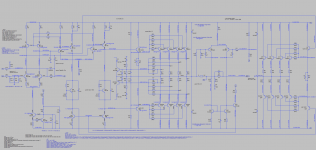
Alright, here is a cleaned up view of my 4 pairs simulation, with info from running the sim.
Protection is disabled. It doesn't work as it should anyway, and that is what basically remains to be fixed.
Load is 8ohms resistive, but I've tried it with complex loads before and it behaves just fine no matter what.
The input is symmetric, and the 2V input brings it right at the onset of clipping.
The power supply is a simple 70V rail to rail. I put a .1ohms impedance and 88mF of filtering, which might be pretty close to real world.
Obviously under load the rails will sag somewhat, and that makes it clip a bit earlier than with ideal rails at 70V. (+-35V, no center tap)
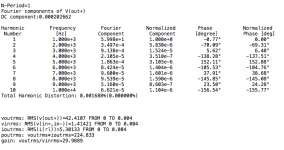
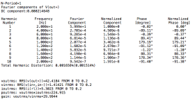
And we get well over 200Wrms output, with a distortion still below 20ppm (@1khz) on that 8ohms resistive load.
I think it's really not bad at all. I'd love to have this work in a real build.
Protection is disabled. It doesn't work as it should anyway, and that is what basically remains to be fixed.
Load is 8ohms resistive, but I've tried it with complex loads before and it behaves just fine no matter what.
The input is symmetric, and the 2V input brings it right at the onset of clipping.
The power supply is a simple 70V rail to rail. I put a .1ohms impedance and 88mF of filtering, which might be pretty close to real world.
Obviously under load the rails will sag somewhat, and that makes it clip a bit earlier than with ideal rails at 70V. (+-35V, no center tap)
And we get well over 200Wrms output, with a distortion still below 20ppm (@1khz) on that 8ohms resistive load.
I think it's really not bad at all. I'd love to have this work in a real build.
Attachments
Standard VI limiting is going to behave wonky in this circuit. You’re using a single error amplifier for both sides of it, and shunting one sides’s VAS transistor is going to try to force the other side to compensate. Unless everything limits at once, symmetrically, it’s goiing to fight itself internally. You’re probably better off abandoning traditional load line limiting, and using a current transformer in the output to sense overload. Then drop the gain back at the input of the amp. The big monster Crest class H amplifiers do it this way, and some modern Crown models do as well.
Yes, that's the issue I've been fighting with. The limiter can't do its job right because everything fights against it while it's trying to act.
I tried various things to attempt to make it work, I even added a transistor on each of the vas (both) to sense when they strain from the protection acting and tried short circuiting the drive to the vas at their bases. I couldn't make it work right.
I'm also thinking one thing to try would be to not act on the vas and the bases of the drivers, but rather directly pull the rug from under its feet directly at the input stage by suppressing the bias current from the input diff stage.
Although it's a bridge and the 2 sides each have outputs, drivers and their own vas, there is only a single input stage to drive everything.
Once this is figured out, this amp should work great with a properly working protection.
Adding a current transfo on the output would add some extra inductance and resistance, which would change things quite a bit, and only the current would be taken into account and ignoring the SOA. I'm not sure how this could be done right without bringing in something that reduces performance.
The output stages are very robust with 4 pairs, with loads of SOA, and with the protections limiting excesses, the output stages should be able to handle a 2ohms load on each side, which would allow a 4ohms load on the amp, which means a bridged bridge could drive a normal 8ohms load and get plenty of power.
I simulated a 5 pairs as well, which would definitely handle the bridged bridge with the 8ohms load, fairly comfortably. But for now I'm not aiming at the power freaks seeking unreal amounts of power, just the "normal" amount, in this case near 220W/8ohms on a single grounded bridge.
So the question is, if keeping the VI sensing method for proper SOA protection, but making them act on the input stage instead of trying to fight internally, can that be done?
Should a new thread be started for this?
This still definitely falls within the main topic of 2n3055 based amps for this existing thread, but maybe it deserves its own thread.
This is an unusual design, rather unique and I don't know of any actual builds ever made this way.
It's a "bridgeable grounded bridge". With power capabilities rarely seen using only 2n3055 type outputs and rails not exceeding 70V rail-to-rail.
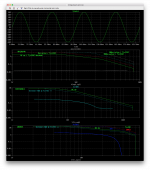
I pulled up the SOA plots on this last sim (4pairs bridge). Loaded with resistive 8ohms, and looking at the bd140 high side vas transistor, the mje15030 that follows and the 1st 2n3055 after that (the others show the same usage).
The amp loaded at 8ohms resistive, actually loads each side at 4ohms, and the 4 pairs are spreading out that load current nicely to a rather low level per output.
This is at max power, right at the onset of clipping. Protections are disabled. Frequency was 20hz. Input level 2V.
Well within the SOA, with reserve area for more complex loads, and hopefully enough to handle the cases when the limiter is acting.
Attachments
I took the time to double check major sources for the 3055/2955, and they're still active by several manufacturers and available near several reputable suppliers. And I even chatted with an agent from arrow.com, specifically on the subject of fake parts. The agent assures that they only provide genuine stuff. but this doesn't really remove all the wariness.
I guess a test sample would be a thing to do. Just in case.
But those parts are definitely still around and if the issue of fakes can be managed, this can be done.
I also looked at my old stock of over 30 older 3055 and at least 40 2955, which I tested for second breakdown and marked them. Almost all of them had a second breakdown over 120V, so without pushing too much over the 60V datasheet specs, like a few volts as on such a design as the grounded bridge, it should be fine. But just in case it's still a good idea to test all parts first for second breakdown.
I also looked at my old stock of over 30 older 3055 and at least 40 2955, which I tested for second breakdown and marked them. Almost all of them had a second breakdown over 120V, so without pushing too much over the 60V datasheet specs, like a few volts as on such a design as the grounded bridge, it should be fine. But just in case it's still a good idea to test all parts first for second breakdown.
Bonjour Spookydd,
Could you please show how to check for second breakdown, practically?
Thanks & cheers,
Jacques
I simply used a meter that has that feature. I don't know of many, as they aren't that common that can do this, but the one I used is the DUOYI DY294 meter.
It's a very tricky thing to do usually, because it can very well lead to the destruction of the part measured, but it is possible to do so non-destructively (very carefully).
I looked at a patent on this issue, which was too hard to make heads of tails of. Patents are written in an extraterrestrial language that only the initiates can understand.
Still there is a method and it works.
I forgot how much that meter was, but it's not something to break the bank. I'm sure you could find one on ebay sometimes...
PDF app note concerning transistor breakdown.
https://www.onsemi.com/pub/Collateral/AN1628-D.PDF
It looks to possibly be a destructive test to me from inspection of the trajectory of the V-I curve in Figure 4.
The curve looks like a voltage sweep to me and breakdown voltage sweeps are prone to runaway current that can be destructive.
In order to know if the test is destructive, you would have to carefully and fully characterize the device, then perform the breakdown test and then repeat the initial characterization.
I was just looking again at that pdf from onsemi. I've had that for some time.
The thing is, manufacturers do test their devices as part of their manufacturing processes, and they even classify devices according to those measurements. So obviously it is feasible to do such tests non-destructively.
From what I gather, to make sure there is no destruction, one thing that's done is to make certain the current doesn't get high at all. That meter that I mentioned, keeps the current below 1mA.
If you’re keeping the current at 1mA you’re not testing second breakdown - you’re just testing vceo. 3055 rated at 60, 15015 rated at 120, and almost all pass 120. Surprise, surprise.
To test 2nd breakdown, you need to pass 2.87 amps with 40 volts vce, while maintaining the case at or near 25C. I do the test by rigging it as a current source with a large emitter resistor to set the current and a convenient voltage at the base (say 12 or 15 volts). Put it on a big heat sink, and run Vce up to 40 or wherever. Genuine devices will hold. The good news is that even generic parts would pass this, if it has a real 115 watt die inside. 40 volt s/b is not that hard for any linear amplifier transistor. Switching types often have trouble with it.
The 2N3055A or the old RCA hometaxial types would handle full power all the way to 60 volts (or beyond). You don’t really need that capability in your design - the 40 volt second breakdown is fine with the lower rail voltages.
I was just looking again at that pdf from onsemi. I've had that for some time.
The thing is, manufacturers do test their devices as part of their manufacturing processes, and they even classify devices according to those measurements. So obviously it is feasible to do such tests non-destructively.
From what I gather, to make sure there is no destruction, one thing that's done is to make certain the current doesn't get high at all. That meter that I mentioned, keeps the current below 1mA.
I think that you may be mixing metaphors. Production parts are tested for functionality and or parametric test/extraction. Not reliability. Reliability testing happens in a different room with different equipment by different people. Reliability testing is a do-it-once-and-you-are-done sort of thing whereas functionality and/or parametric testing is performed on every lot. Reliability testing can be 100X to 1000x and beyond more time consuming than production test so it is not possible to perform reliability testing on every production lot.
For some devices, breakdown is a parameter and is specified in the datasheet. There are devices on the scribe lines between dice that are used to characterize the wafer and the process. Capacitors on these scribe lines are sometimes tested destructively for breakdown for purposes of a datasheet spec. If you integrate the current over time you get charge. Charge-to-breakdown (QBD) is an industry standard test.
These are my first-hand observations having been in a number of wafer fabs for my day job working with all of the types of engineers described above in the performance of the tasks described above.
Have a close look at the breakdown curve in Figure 4 of the app note. The Y-axis is current. Second breakdown happens at what looks like very high current and the slope of the line is essentially infinite. That looks like a destructive breakdown test to me and I have observed those types of tests on devices on a wafer with expensive test equipment.
My intention is to just share some info. I am not casting any aspersions on anyone's knowledge or skills. Just participating in a discussion.
cheers
- Home
- Amplifiers
- Solid State
- Amplifier based on 2N3055