In my experience, taking signal ground from the PCB to input jacks and from there to star central ground makes the amp less sensitive to stray fields inside the case - e.g. from power transformers. Your topology works too, even may be better if input jacks are isolated from chassis and do not share a common ground tab.
In case you use split power for stereo, this is of no concern. For 2 or more channels, I prefer to take the signal ground "star" center to the input terminals and to distribute it from there to all channels.
In case you use split power for stereo, this is of no concern. For 2 or more channels, I prefer to take the signal ground "star" center to the input terminals and to distribute it from there to all channels.
BTW: even toroids may have a significant stray field around them. When running the cables inside the chassis, I always make sure that all cabling runs along the same side of the transformer (s), never around it in a loop! Additional screening around the transformer sometimes helps.
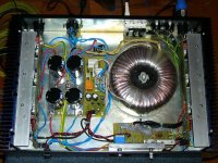
See this picture as an example:
(the mechanical aspects of amp design and cosmetics are NOT my strenghts, so, please do not comment them. This amp has a S/N >126dB, regardless of its "unglamorous" looks - en<20uV at output, ref 250Wrms/8).
See this picture as an example:
(the mechanical aspects of amp design and cosmetics are NOT my strenghts, so, please do not comment them. This amp has a S/N >126dB, regardless of its "unglamorous" looks - en<20uV at output, ref 250Wrms/8).
Attachments
darkfenriz said:Thanks Mike very much
do you use 47nF and 10ohms or different values?
I still use 4.7R + 47nF, it worked well. I don't know which are the perfect values...
Mike
Change your SPICE time stepsize
I think that what what you are looking at ("distortion)") is simply a SPICE interpolation artifact. Reduce your maximum step size in your transient simulation configuration and the sine wave will start to look a bit prettier. Not too small, because the simulation time will of course increase proportionally.
I think that what what you are looking at ("distortion)") is simply a SPICE interpolation artifact. Reduce your maximum step size in your transient simulation configuration and the sine wave will start to look a bit prettier. Not too small, because the simulation time will of course increase proportionally.
Hi Apd,
Would you care to write up your project so we can learn how to try and achieve similar noise and hum performance? And maybe how to measure it.
Rt,
how do we decrease the step size?
this a a glorious achievement.amp has a S/N >126dB, regardless of its "unglamorous" looks - en<20uV at output, ref 250Wrms/8).
Would you care to write up your project so we can learn how to try and achieve similar noise and hum performance? And maybe how to measure it.
Rt,
how do we decrease the step size?
Feedback Loop
Woops!. I guess you already had the answer for SPICE time step sizing. I'm still getting used to the user interface here. Just joined the forum...
Okay, here some suggestion on where to add vitamine "C" to make your amplifier healthy:
2. Bypass capacitor from your power rails (30V) to ground are mandatory. Use ceramics for their low ESR. 1nF to 100nF are required, after the 22 Ohms supply line resistors. Watch the voltage rating of the caps! If your circuit is "large", use them in multiple locations in your circuit, even before the 22 Ohms resistors. Make sure they are close to the components and keep the "loop area" small. That is: Imagine a loop from the supply rail through the amplifier to GND and then back through the cap. Use them both on the positive and negative rails; equally sized.
2. The 100pF capacitor in your feedback network is in fact advisable. In fact, with 22kOhms and 100pF, you put a pole at 72kHz or thereabouts. Reduce that to 30kHz or so, ~330pF or so. This should not destabilize your amplifier. To ensure this, follow #3:
3. Make sure your amplifier's open loop gain drops down after 30kHz. You do this by inserting a "dominant pole" in your amplifier circuitry *inside* the feedback loop. That is why cranking up the input capacitor does not make a difference for stability!. Increase C1 more and more. C6 is another candidate. I suggest you run a square wave into the amplifier, ~1kHz. Look at your ouput signal (without a long wire) and observe ringing at the edges with a scope. Ringing hint toward instability. Keep upping the capacitors until it goes away. Do not overcompensate. Check the audio bandwidth afterwards.
4. If all this does not help, another compensation point can be added on the tailed pair. Add a 2.2k resistor on the collector of Q2. (would have been advisable anyway for symmertry reasons, but whatever...) Place a resistor in series with a small capacitor between the collectors of Q1 and Q2. Start with 1 kOhms and 22pF. Start increasing the caps until stability is achieved.
It is best to pick one of the 3 methods and JUST use that point to add the dominant pole. Not all 3. Don't overcompensate, or else the slew rate of the amplifier will be compromised, resulting in HF audio distortion. You can see this happen if the THD rise with frequency excessively. At 20kHz, a sine wave will look more and more like a triangle wave. C1 is my "favorite".
The reason why your amplifier oscialltes with a cable attached is that you effectively add a capacitor and thus extra phase shift. You reduce your phase margin. Amplifier go unstable with capacitors, not with inductance. Your speaker looks like an inductance to the amplifier. Hence, to check for stability after you take the above approach, deliberately add caps to the output. Start with 100pF and step it up slowly to see where the square wave starts showing problems again. This should be done with the load attached in parallel, e.g. a 8 Ohms resistor for now (less loud...") You be able to add 50 to 100nF with little ringing. Above that value, you may start to expect some issues.
You be able to add 50 to 100nF with little ringing. Above that value, you may start to expect some issues.
Woops!. I guess you already had the answer for SPICE time step sizing. I'm still getting used to the user interface here. Just joined the forum...
Okay, here some suggestion on where to add vitamine "C" to make your amplifier healthy:
2. Bypass capacitor from your power rails (30V) to ground are mandatory. Use ceramics for their low ESR. 1nF to 100nF are required, after the 22 Ohms supply line resistors. Watch the voltage rating of the caps! If your circuit is "large", use them in multiple locations in your circuit, even before the 22 Ohms resistors. Make sure they are close to the components and keep the "loop area" small. That is: Imagine a loop from the supply rail through the amplifier to GND and then back through the cap. Use them both on the positive and negative rails; equally sized.
2. The 100pF capacitor in your feedback network is in fact advisable. In fact, with 22kOhms and 100pF, you put a pole at 72kHz or thereabouts. Reduce that to 30kHz or so, ~330pF or so. This should not destabilize your amplifier. To ensure this, follow #3:
3. Make sure your amplifier's open loop gain drops down after 30kHz. You do this by inserting a "dominant pole" in your amplifier circuitry *inside* the feedback loop. That is why cranking up the input capacitor does not make a difference for stability!. Increase C1 more and more. C6 is another candidate. I suggest you run a square wave into the amplifier, ~1kHz. Look at your ouput signal (without a long wire) and observe ringing at the edges with a scope. Ringing hint toward instability. Keep upping the capacitors until it goes away. Do not overcompensate. Check the audio bandwidth afterwards.
4. If all this does not help, another compensation point can be added on the tailed pair. Add a 2.2k resistor on the collector of Q2. (would have been advisable anyway for symmertry reasons, but whatever...) Place a resistor in series with a small capacitor between the collectors of Q1 and Q2. Start with 1 kOhms and 22pF. Start increasing the caps until stability is achieved.
It is best to pick one of the 3 methods and JUST use that point to add the dominant pole. Not all 3. Don't overcompensate, or else the slew rate of the amplifier will be compromised, resulting in HF audio distortion. You can see this happen if the THD rise with frequency excessively. At 20kHz, a sine wave will look more and more like a triangle wave. C1 is my "favorite".
The reason why your amplifier oscialltes with a cable attached is that you effectively add a capacitor and thus extra phase shift. You reduce your phase margin. Amplifier go unstable with capacitors, not with inductance. Your speaker looks like an inductance to the amplifier. Hence, to check for stability after you take the above approach, deliberately add caps to the output. Start with 100pF and step it up slowly to see where the square wave starts showing problems again. This should be done with the load attached in parallel, e.g. a 8 Ohms resistor for now (less loud...
You be able to add 50 to 100nF with little ringing. Above that value, you may start to expect some issues.Reducing Step Size
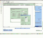
See the attached screen shot. I take it you use ICAP/4 or so, given you simulation pictures. Go to the "Action" drop down menu and select "simulation setup". Then click the transient button and reduce the value in the "Data Step Step". The "Maximum Time Step" is to slow down SPICE if "nothing much is changing", but will not necessarily slow down you simulation. And the latter value should be equal or larger than the first.
If you were using Orcad PSPICE, it is similar. You can find a similar panel in the "Simulation" drop down menu, select "Edit profile" and click on "transient". You will see something similar.
Attachments
Andrew (T)
Surely you know how to make such measurements
The quote is s/n ref. 250W (remember that)
You simply run the very expensive test equipment and the amplifier under test from low noise d.c supplies or car batteries as some of us call them – You make the measurements in a special enclosure (chicken coop) with yourself outside but even so you hold your breath and clench your buttocks just in case. Slightly better performance can be achieved if the power generating authority in your area can shut down the grid while you measure.
Other methods could be to use all the filters the test equipment has and to make the measurement at a frequency say 20 kHz such that all harmonics are sufficiently attenuated but even if I do that with my HP analyser in series with my old Tektronix AA501 I still cannot get better than –120dB unbalanced! However I can make a 100W amplifier with s/n better than 100dB which sounds fantastic - does that count ??
Regards to all
Keith
AndrewT said:Hi Apd, this a a glorious achievement.
Would you care to write up your project so we can learn how to try and achieve similar noise and hum performance? And maybe how to measure it.
I hope no one is disappointed:
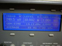
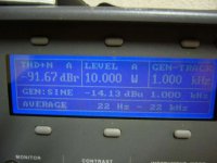
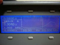
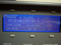
measurements quoted are done with an Audio Precision Portable One analyzer, running from its standard mains supply. So does the amp - as pictured. True: the screen of my laptop generates some RF interference when nearby, so I usually keep it at least 2m away when doing such measurements.
The Portable One analyzer has a 92dB dynamic range within each measurement interval, however, when comparing absloute levels, a much higher effective measurement range can be achieved.
This translates into English as follows: the Portable One cannot measure THD+N lower than -92dBr in respect to an actual output signal (when present), however, it can measure reliably microvolts when a 'main' signal is not present - i.e. noise threshold, noise spectrum, etc.
The specific circuit referred to in this example runs off +/- 70Vdc, and its 'idle state' output noise is about 20uVeff (10Hz-22kHz, unweighted) @gain =70 (+37dB). Relating that noise level to its unclipped rms output voltage at full power with its typical supply (~42Vac), S/N>126dB.
The voltage limits of the circuit are +/- 145Vdc, without supply rail switching, which would render an even higher value for its dynamics capabilities (>130dB).
@AndrewT: I will consider your proposal and may post circuit details in a new thread.
If you pay attention to cabling routes and follow EMC trace layout rules, any circuit would render its peak performance.BTW: What would be the point of making measurements in an "artificial" setup that would not be applicable in "real-world" applications later... just for a pat on the back??? No, thanks! Not me...
AndrewT said:Hi,
so how did you measure 20uVac from DC to 20kHz bandwidth?
Did you amplify the noise signal first then measure or what?
Spell it out for me, please.
Just hook up the analyzer to the idling output and take a direct voltage measurement, specifying the bandwidth from the menu.. It will calculate and display the rms voltage value.
I guess you don't have one handy, so a very crude setup could be done with a scope, whose sensitivity is at least 1mV/div. Make a simple low-pass RC filter with its -3dB point around 25kHz, resistor value <1kOhm. Connect the probe at the filter output, and in my case - the reading is a straight line, ripple barely noticeable. Another very crude, but effective method of subjective noise evaluation is to connect a tweeter at the amp output and listen.. ideally the tweeter should be "dead", hiss barely noticeable in a very quiet room, when your ear is stuck to it.
Andrew (T)
My cheeky statement - "The quote is s/n ref. 250W (remember that)" — Was NOT for fun — cynical maybe but I hope also thought provoking!
As it turned out the measurement given was simply – Noise referenced against a 250W equivalent voltage – Not THD+N or Noise measured in the presence of a signal at 250W or better still signals. But simply a projected figure for residual noise.
ApD
With the equipment you mention the measurement was most likely a highly averaged reading — adjusted by maths to give the answer? Exactly what you would refer to as an "artificial" setup that would not be applicable in "real-world" applications later"
When your amplifier is in operation — even at less than 250W — there will be large signal and mains currents circulating and the s/n should be nearer to what one would expect in practice.
May we ask for the peak THD+N at say 1W, 3.16W, 10W, 31.6W, and100W. These readings may be more revealing if not as sensational
May not reply for a while as I must fly but I will look in when I can
Keith
dcd said:Andrew (T)
My cheeky statement - "The quote is s/n ref. 250W (remember that)" — Was NOT for fun — cynical maybe but I hope also thought provoking!
As it turned out the measurement given was simply – Noise referenced against a 250W equivalent voltage – Not THD+N or Noise measured in the presence of a signal at 250W or better still signals. But simply a projected figure for residual noise.
ApD
With the equipment you mention the measurement was most likely a highly averaged reading — adjusted by maths to give the answer? Exactly what you would refer to as an "artificial" setup that would not be applicable in "real-world" applications later"
When your amplifier is in operation — even at less than 250W — there will be large signal and mains currents circulating and the s/n should be nearer to what one would expect in practice.
May we ask for the peak THD+N at say 1W, 3.16W, 10W, 31.6W, and100W. These readings may be more revealing if not as sensational
May not reply for a while as I must fly but I will look in when I can
Keith
My apologies to the owner of this thread for spamming, as we have drifted away from the original question.
Keith, a picture is worth 1000 words. I have not taken screen - shots at all power levels you mentioned (as this was never an intention)... but maybe the pics may help you guys in the UK realize, that other people in other places have at least a rough idea of what electronics and audio is about:
(and please note the device's design limitations, as listed in its specs, http://www.audioprecision.com/index.php?page=products&id=1000001011)
Wish I could get my hands on one of their better units..
Circuit revisions
Dear Zeus_threat
It' s amazing what some insomnia does for DIY fans..!
Let's get back on track with your circuit.
I took the liberty of simulating your circuit, and doing some minor adjustments to it. Here's what I found, and what I changed:
1. The currents in the input diff. amp are unequal. You don't want that. A quick "fix" would be to change the value of R3, however, a better way is to introduce a new resistor R3a (22-100 ohm) in the emitter of your voltage gain stage Q3. This has a number of advantages:
- reduced thermal drift, as currents in Q1/Q3 would remain at a fairly constant ratio, and as a consequence the thermal drift of the output offset voltage would be mostly uninfluenced by temperature;
- introduces some local NFB on Q3, improving phase margin and stability.
Its value is somewhat dependent on the transistor types you use in your real circuit and will influence open-loop gain. Adjust R3 to get equal currents in the diff amp - not by measuring the voltage drop over R1, R2, but rather equalize the resistors in the DC feedback loop and input bias (R10+R10a=R11+R10b) and adjust R3 for zero output offset voltage. A pot in series to R3 would be very convenient.
2. A new resistor R10a + C4 have been added to the input, C4 provides a HF return to ground for proper operation of the diff amp, R10a helps reduce RF interference. You can play around with the values to reduce the maximum slew rate of an input signal, which also may improve TIM and IMD.
3. To maintain symmetry, another resistor R10b has been added to the other base. It is optional, to make the DC loop equal value on both sides for minimum output offset (assuming equal currents and gain-matched, thermally coupled Q1, Q2).
4. R23, R24 don't really do much for you, especially R24, as it is feeding the CCS. Supply ripple will have no practical influence on the CCS performance. You can keep R23, with caps to ground on both sides to improve supply ripple rejection in the voltage amp stage. Do not connect them to signal ground!
5. R5 seems a bit too high for proper operation of the Vbe multiplier. I assume you would place a pot there anyway, so as to get the right idling current. Place the pot in place of R5, so as to shut-off idling current in case of a bad pot. Usually, it's better to place both a pot (as a variable resistor) and a fixed resistor in series, so as to reduce the adjustment range of the pot.
6. A cap C6a has been placed across the Vbe multiplier, between the bases of the driver stage. Mandatory. There's little, if any benefit from C6 in your version. See the output waveform with square waves with and without the cap...
7. R19, R20 - optimize their values on the real model, possibly also by adding caps b-c on Q5, Q8. In some cases, slight oscillations might occur during one or both halves during large voltage swings. Adding these resistors + caps removes that, but if the resistors are too big, they would compromise open-loop output imperance and the current drive capability of the circuit.
8. Keep C1 as low as practical. The faster your voltage gain stage, the better. Slowing it down reduces open-loop gain and increases distortion at higher frequencies. You don't want that. A typical setting would be to keep slew rate above 20 and below 50 V/us (SR~Ic(Q3)/C1). The type of capacitor has been reported to influence sound quialty, so use a NP0 ceramic or polyester type, ot whatever makes you happy, just look out for its voltage rating.
9. Do all your "fiddling around" without a coil and RC network at the output. Once you get the circuit to work properly without any oscillations, add them at your discretion "to be on the safe side", if you prefer. Check for "ringing" with a 1kHz square wave input and capacitive load. Ideally, the output waveform should change just slightly at the rising and falling edges with a 2uF cap connected at the output. Proper grounding topology is critical. Tackling oscillations with an RC network at the output is like cleaning by sweeping dirt under the carpet. Use it as a last resort, if all else fails.
10. I assume you've separated the input and output grounds, providing a separate connection for each to "star" ground at the p/s. If you add any filter caps, make sure they are not grounded to the input ground. Keep that as "clean" as possible. Only the input and FB components should be connected to it. An optional resistor RG (~10-20 ohm) could link them on your pcb, but be very careful with it. Its function is to "lift" signal ground from the chassis ground, typically connected to central ground, and it's location should be near the input terminal ground pin to chassis.
11. On FFT simulations, THD@1kHz is about 0.05% with a dominant third harmonic. One way to reduce it would be to hike the open-loop gain by reworking the diff. amp with a current mirror - a pair of transistors in the collector circuits, thus increasing overall feedback. Another cause is the non-linear change of h21 of the output transistors with increasing load current, which you can improve by adding more output devices in parallel. The benefit is reduced open-loop output impedance and higher power/current capability. The added cost of a pair of output devices is negligable, the returns are quite obvious.
12. Is there a special reason to put a BD140 as Q3? Both Q3 and Q10 will dissipate around 120mW average, so you could try with BC556B in place of BD140. It is faster and has a higher h21, but at +/- 30Vdc you would be pushing them to their voltage limits. MPSA42/92 of BF422/423 would probably do a better job.
13. Amps without any form of protection are an invitation for disaster - speakers cost more than transistors...
Hope these notes will help you build a good amp! I'll attach the revised circuit.
Best,
Attachments
Hi,
R10a and C4 have a 0.01uS time constant.
I would increase RC by a factor of 50 to 150.
What effect will this have other than the simple filter?
R18 to power ground?
Is this introducing artefacts into the CCS?
How about splittng R18 and taking a cap from split to -ve rail?
Or
connecting R18 to clean ground?
I just copied your post into notepad and saved it. Thanks.
A pot in parallel would be better. To be replaced by a fixed resistor on the back of the PCB if there is no room in the layout.A pot in series to R3 would be very convenient
R10a and C4 have a 0.01uS time constant.
I would increase RC by a factor of 50 to 150.
What effect will this have other than the simple filter?
R18 to power ground?
Is this introducing artefacts into the CCS?
How about splittng R18 and taking a cap from split to -ve rail?
Or
connecting R18 to clean ground?
I just copied your post into notepad and saved it. Thanks.
- Status
- This old topic is closed. If you want to reopen this topic, contact a moderator using the "Report Post" button.
- Home
- Amplifiers
- Solid State
- Amp distortion